This thread has been locked.

If you have a related question, please click the "Ask a related question" button in the top right corner. The newly created question will be automatically linked to this question.

INA302: Schematic design and Layout review

Part Number: INA302

Hi Team,

I am designing a Bidirectional Current sense amplifier, with ALERT output.

Specs:-

Bidirectional Current sensing with ALERTx transparent mode

Max 30A in one direction, 70A in other direction, with RSHUNT = 0.75mOhm

I need ALERT output in only one direction.

I put option for keeping INA302 at VREF of 1V or 1.25V depending upon testing using Voltage Reference IC MCP1501.

I connected the OUT pin with RC filter to ADC input of my MCU ATSAMC21G18A and ALERT1 and ALERT2 pin on MCU interrupt pin.

Please review my schematic, let us know your valuable comments.

Also I want review my PCB layout, but I don't know which file format to share, please guide.

Please let me know in case you need more info regarding application.

Regards,

Avinash

Current Sense Amplifier.pdf

  • Hello Avinash,

    Thanks for posting to the forum.

    There are few things here. The ALERT pull-up resistors should be 10kΩ ideally to match the recommended values from datasheet. See Figure 48 of datasheet.

    The input capacitor C51 should really be directly at the input pins (on right side of 4.7Ω input resistors) to achieve low-pass filtering. See Figure 50 of datasheet.

    Your shunt resistance is actually 0.75mΩ||0.75mΩ = 0.375 µΩ.

    Your PCB may be different, but best practice is for the device decoupling capacitance (specifically C53 to be right at the device Vs and GND pins. See Figure 54 of datasheet. You can also use this to guide yourself on the input pin connections to the shunt resistance, which will be critical for your small shunt resistance. You want to ensure proper Kelvin sense connections to the shunt resistance such that you are not sensing any additional solder resistance.

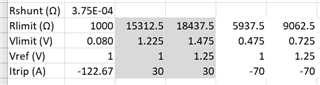
    I am not sure if the 30A is positive and 70A is negative or vice versa, but you will need to revise your limit resistors R79 and R78. Also, the trip current will change when the reference voltage is changed. See equation 3 of datasheet. See below of table using Equation 3 to solve for Rlimit for various VREF and Itrip value combination (spreadsheet is attached).

    Sincerely,

    Peter

  • Hello Peter,

    Thank you for your feedback.

    We have changed values of ALERT pull-up resistors to 10kΩ as per Figure 48 of datasheet.

    Also changed the position of the input capacitor C51 directly at the input pins (on right side of 4.7Ω input resistors) to achieve low-pass filtering. as per Figure 50 of datasheet.

    Sorry that was mistake in schematic, we are using 1mOhm and 3mOhm resistor in parallel, so equivalent shunt resistance is actually 0.75mΩ. Is it fine if you use two different value shunt in parallel ?

    we placed device decoupling capacitance (specifically C53 to be right at the device Vs and GND pins (as per Figure 54 of datasheet).

    We ensured proper Kelvin sense connections to the shunt resistance as per datasheet.

    We also revised our trip current limit resistors values. I think this way our schematic is reviewed.

    Also I want to get review my layout also, please suggest the way i should share. Because I cant share openly on forum (Its confidential).

    Regards,

    Avinash 

  • Hello Avinash,

    Keep in mind the 10kOhm pull up resistor may need to be decreased depending on the speed of your digital communication and capacitance elsewhere on these bus lines.

    For the shunt resistors, yes using different values is fine, but you will want to be careful with the input sense connections. In scenarios with multiple shunt you can have IN+ and IN- traces branch out into two traces each. One branch goes to positive side of 1mOhm and the other goes to positive side of 3mOhm. The same is done for IN- input trace. This is done to effectively average the voltage.

    You can share you PCB information with a private message to my profile here.

    Sincerely,

    Peter