This thread has been locked.

If you have a related question, please click the "Ask a related question" button in the top right corner. The newly created question will be automatically linked to this question.

Additional copper region in OPA361 footprint

Anonymous
Anonymous
Guru 17045 points
Other Parts Discussed in Thread: OPA361

Hi All,


I would like to ask a question on OPA361 footprint.
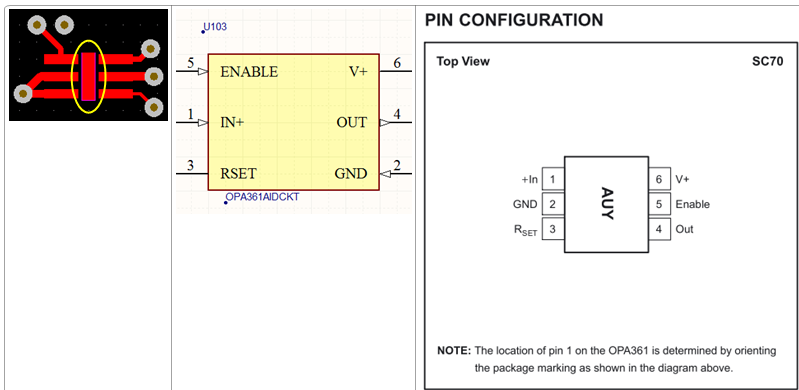


I have found several components have additional, unnecessary copper region with them in EVM6437 PCB file (DM6437 EVM by SpectrumDigital), and that of OPA361 is are shown here.


What are the red regions (circled in yellow) locating within the component footprints? I checked OPA361’s data manual and found it doesn’t require additional copper thermal land (as those for PowerPAD), so I don’t see any reason why these additional copper regions are added.


Could anyone advise me of their use, or that they are actually not needed and I can safely remove them?


Thanks,

Zheng

  • Zheng,

    As you mentioned, the OPA361 does not have a PowerPad, this is confirmed with the device DS and p. 16 of the DS shows a recommended PCB landing footprint.  It is possible that a a generic footprint, one including a thermal pad, for an SC70 package is what has been implemented in the PCB file you have.  You can remove the landing, this will also allow for the possibilty of routing beneath the IC.  Hope this helps.

  • Anonymous
    0 Anonymous in reply to Jared Casey

    Dear jjc,

    I see it, thanks for the confirmation.

    Zheng