This thread has been locked.

If you have a related question, please click the "Ask a related question" button in the top right corner. The newly created question will be automatically linked to this question.

THS4524: analog buffer/fanout is availalbe?

Part Number: THS4524
Other Parts Discussed in Thread: THS4551, OPA862, THS4552, OPA2677, THS4131, DRV1100

Hi, 

I'm designing a test board for our product.

The requirement is to design a board:

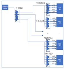
- 1x analog input, differential input (0-10MHz, input Vpp < 1V)

-  32x analog output,differential out, with same bandwidth and same amplitude as the input

- the test board is aimed to check all 32x receive channels are working good.

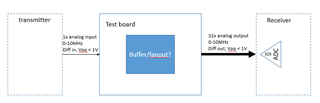
is there analog fanout solution for this requirement?

or can I shift my test stimulus signal to digital signal, for example LVDS. If that, fanout device for digital signal is more easier to find  and lower cost than analog device.

Thanks for your advice.

  • You would need to define your load - do you need to do doubly terminate diff transimission lines, or is this just a cap load where an iso R is needed. 0Hz implies you are testing DC levels into your DUT?

  • Hi Michael,

    Thanks for your reply.

    So far I can confirm is that the ADC in Receiver board is AD9637 from ADI.

    About doubly terminate diff transmission lines,do you mean terminate the diff lines individually ? I do not get your point, please give further explaination.

    About the input bandwidth,  there is no need to test DC level. But the bandwidth upper limit  is 10MHz.

    Can you give some solution for this requirement?

  • So the next question would be what are you testing? If you are trying to do some kind of SFDR test, then the amplifier requirements become more challenging. What do you plan on looking at anyway?

    Also, eventually would need to know where your signal is coming from? I had a kind of similar task some year back to generate a very low MTPS input test signal for multi-channel G.Hn line drivers. Interesting problem in ATE. I did write an article on my solution, but would have to look for later if you end up needing something similar. 

  • I'm testing a chirp signal with bandwidth 0.5MHz - 10MHz.  i.e.  linear modulation of sine wave.

    The chirp signal comes from one DAC followed by a amplifier driver. It seems much simpler than your task requirement.

    Appreciated if you share more information about your solution.

  • Hi Michael,

    Below is my draft concept for this test board. But one THS4524 output need to drive 8  input channels of next amplifier stage.

    I'm not sure about this. Also how to terminate this kind of transmission line ?

    Thanks.

  • Well the difficulty in using FDA's like this is they show the Rg element as an input R. So they all look like a parallel R load to your 1st driver. To raise that, increasing all the R's  gets into noise issues. 

    The quad FDA THS4524 is not particularly small, I also rarely use it due to performance issues we fixed with the THS4551 and dual THA4552

    Do you have board space issues? alternate approaches include 

    1. using Baluns in some way, commonly used in AC interfaces. to ADCs

    2. Differential I/O dual op amps showing high input impedance

    3. A high input impedance single to diff device - there was a recent intro like that, forgot part #. 

    What is the first amplifier driving your chirp? 

    Driving through Montana today, kind of out of touch mostly. 

  • Michael,

    Hope you had a nice trip.

    I have no board space issue.

    why Balun for driving ADC in AC coupling?

    the first amp driving the chirp is ADA4940-1, with the inputs from DAC(AD9705)

  • Hello,

       Here is a good blog post describing what Michael meant with balun vs FDA. For Michael's third point I believe he is talking about OPA862. Are you looking for any gain for any of these channels?

    Thank you,

    Sima

  • Sima,

    thanks for your sharing. I'm looking on it.

    the input and output are both diff signal , so I think it's no need to pick single-end to differential solution.

    I have no gain requirement for these channels.

    The 32 output channels copy the input channel. I'm finding a low cost solution for this ,but no board space limit.

  • Morning jkw

    So eventually you do have a fanout issue. Paralleling a bunch of FDA's puts all their input resistors in parallel

    1. I assume you want to do a single 5V solution

    2. For a good 0.5MHz to 10Mhz test signal target about 100kHz to 50MHz signal span in the interface

    3.the AD9637 quotes max input of 2Vpp - that is 1V in each polarity. (usually -1dBFS test or 1.8Vpp max, 0.9Vpeak)

    First, here is an intermediate 5V stage that can drive a lot of output current into the parallel final FDA's (which are very useful for CM control) from here, no further AC coupling is required. If we imagine a target. If we want to limit the demand to 100mA for a 0.9V peak across all the parallel input R's, we can get down to 9ohms load, target a minimum R of 20ohm to be sure. Then, targeting 1kohm for the Rg values in the ADC's we can drive 50 of those in parallel with this stage, hopefully enough. This ckt sits at 2.5V DC, then the ADC Vocm will drive the FDA input Vocm which will set up a DC level shift current as well. You should probably only need one of these to provide the fanout to all the FDA stages, but you can add a 2nd with these R values and the ADA4940 can drive that easily

    Then, all the FDA's in parallel (I would use the dual THS4552 with 1kohm R's) will drive the ADC's in test - the FDA outputs will be DC coupled with the Vocm shifted to the ADC value - add a simple RC interface to bandlimit to 60MHz - I would say a 100pF differential only with 2 series 13ohm  into each ADC path - need to lay that out with low C parasitic in the traces from the OPA2677 output to each RC input. 

    Incidentally, here are the example interfaces from the AD9637 - almost always baluns to get the best SFDR plots. 

    And the OPA2677 sim file I am using - original transistor level model by Rea Schmid, 

    OPA2677 inverting buffer.TSC

  • Going a bit further looking at the DC level shift current for the CM control, 

    Operating the OPA2677 midscale DC to get the best headroom on the signal - 2.5V here, 

    The AD9637 wants to se a CM input (provided by the FDA control) of 0.9V. 

    If we use 1kohm Rf = Rg, each FDA shows an equivalent 2kohm load from 2.5V output DC from the OPA2677 to the 0.9V output DC Vcm for the ADC inputs. Hence each side of each channel needs a DC level shift current of 1.6V/2kohm or 0.8mA on top of the signal current needs. 

    Looking at the 5V spec table, say a for sure 150mA output is available from the OPA2677 (0C to 70C Tj). So we can drive quite a few of these in parallel with a single OPA2677

  • Hi Michael,

    sorry for the late reply.

    I'm simulating your solution in Pspice for TI. But there is no THS4551 mode in the Pspice for TI. so I chose THS4131  for instead.

    In the simulation project, OPA2677 + THS4131  combination is simulated with 8 channels output. I attached the project file if you are interested.

    Another thing, in real situation, I have to use single 3.3V power solution. So THS4131 is not suitable based on power requirement and another thing is the chip consumes too much current, while THS4551  is ok.opa2677+ths4131.zip

  • The THS4551 has a PSPICE model, it is under design and development tab - in this introduction I had generated TINA files for all the data sheet circuits so that clutters up that listing, but if you scroll down you will find this to download. Also, the OPA2677 will need 5V supply even if you use 3.3V on the THS4551. 

  • Thanks, Michael.

    I will redo the simulation with THS4551 model.

    But for the OPA2677 requiring 5V supply, any device with similar performance supporting 3.3V supply can be recommended?

  • Have you settled on the FDA resistors and how many in parallel need to be driven but the OPA2677 outputs. 

    So for higher current output you normally go with Class AB output stage like the OPA2677 which requires more headroom to the supplies, without  looking I think the OPA2677 is about1.2V with heavy load. So on single 3.3V supply, you lose 2.4V to headroom and would only have about 1.1Vpp swing left, if the part operates at all. 

    These high output, higher speed devices, came out of xDSL line driver requirements - there are only 2 RRoutput type ones I can think of right now, 

    1. TI DRV1100 - it is a CMOS device and shows NRND pointing to the OPA2677 (I am surprised it is still available).only operates down to 4.5V

    2. An ADI device that I cannot remember right now - not sure it is spec'ld for 3.3V as very few DSL line drivers need that. 

    Not sure why you cannot provide 5V supply, if thier outputs are going through 3.3V supplied THS4551s, the FDA outputs to the ADC's cannot go beyond 0 and 3.3V. 

  • For FDA resistor, Rf and Rg are set to 499 ohm. And totally 32 FDA  in parallel needs to be driven by OPA2677

    About single power supply, the test board we are designing is powered by the upstream board(transmitter side) with one cable, the power is integrated in this cable with 3.3V, so I have no other choice for this power.

  • So back to your Fanout question - really a current drive question, your 32-499ohm are in parallel showing an effective load of 15.6ohms if driven in parallel - say we are trying for +/-0.45V on each side into the FDA's, that is 29mA drive - not really too much I suppose. 

    But, if you need to get by with only 3.3V supply, then a RRoutput is required and the OPA2677 cannot be used. 

    Linear output current is difficult to specify, but here the ADA4940-1 on 3V makes an effort and shows typ 38mA - no idea what is the minimum, a gap in the specs. 

    Also, directly loading the ADA4940 with what looks like 15.6ohm on each side will probably get into its AC response possibly making it unacceptable. We put more efffort into that on the THS4551 specs, where here is the 3V table on linear output current, And this is a final test spec - only DC testing is done at final, but better than nothing (and better than the ADA4940 effort

    Maybe what you should do is drive two parallel THS4551 stages out of ADA4940 then have each of those two drive 16 each of the final ADC drivers. then each will see 32ohm on each ouput line, still a pretty heavy load but you can expand this concept if need be.