This thread has been locked.

If you have a related question, please click the "Ask a related question" button in the top right corner. The newly created question will be automatically linked to this question.

OPA991: OPA991 is not meeting its slew rate specification.

Part Number: OPA991
Other Parts Discussed in Thread: LM7301, TINA-TI, TLV172, OPA172, OPA2991, OPA2990, OPA990, THS4561, THS4551, THP210, TLV2172

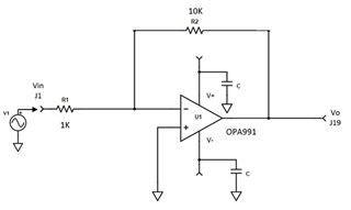
I have been using the LM7301IM5 op-amp and switched over to the OPA991 as your web site suggested as a better part. In the same circuit, the 7301 meets its slew rate spec of 1.25V/us and works well. I ordered Qty 100 of the OPA991 on order number XXXX and each one I have tried is giving me a slew rate of 0.45V/us not the 21V/us shown in the spec. and the output is very distorted. The circuit is a basic inverting amp with an input resistor of 1K ohm and a feedback resistor of 10K ohm giving a gain of -10V/V. The supply is +/- 15V and the non-inverting input is grounded. With a sine wave input of 0.5V volts for an output of 5V at 50KHz the output is very distorted and trapezoid looking. To show that the board parasitic were not to blame, I dead bugged all the parts on top of the OPA991 completely removing the board layout. The board only supplied power at this point. The output of the OPA991 was still distorted. Again, the LM7301 works fine in the same circuit. I have now tried 10 of the 100 parts I ordered and they all act the same. Could have I been sent the wrong part? The parts are marked O91V which looks correct? I need help! any idea what could be going on? This is supposed to be a better part, could I be doing something wrong? It is a very basic circuit. Thanks for your help with this!

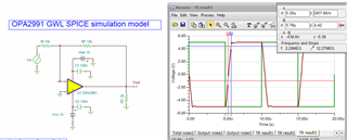
This is the simple circuit below.

This image below shows the slew rate of the OPA991, the input is a 0.2 volt square wave. Same circuit as above. The image is the output. It shows a 0.533 V/us slew rate, not 21V/us as the spec shows. I have multiple parts that are doing this. Hope this helps?

Here is another screen capture of the scope image for the OPA991. Yellow is input, Blue is output. You can see the output distortion and it does not have the proper output gain. Input is a sine wave at 50KHz @ 0.5Volts peak (Yellow), output (Blue) is something less than 5V. At a gain of 10 it should be ~5Volts peak. Thanks

  • Hi Lidong,

    see the test condition of slew rate specification: Vs=40V and G=+1.

    It's quite usual for an OPAmp that the slew rate decreases when demanding a gain of G=+10 instead of G=+1.

    Kai 

  • Hi Lidong,

    The OPA991 has slew boost circuitry to increase the slew rate of the device up to 21V/us. There must be a large signal applied to the inputs to turn on the slew boost circuitry. A 0.5Vpp amplitude is not enough. I recommend taking a look at our TI Precision Lab Videos on Slew Rate for more information. Specifically Video #3 discusses small signal vs. large signal behavior.

    Thank you,

    Tim Claycomb

  • Hi Tim,

    Thankyou for responding to my question. The TI Precision Lab Videos were a great help in understanding.

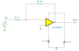
    But I still have an issue. I have simulated this simple circuit on TINA-TI and PSpice. I have also worked out the equations found in the TI’s “Analog Engineer’s Circuit Cookbook: Amplifiers” Page 9 Inverting amplifier circuit.

    All three show that the 50KHZ circuit, which I have sent you screen shots of should work and not be distorted as shown. The simulations also show quite different square wave response.


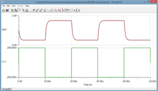
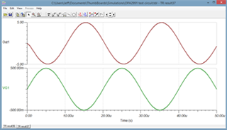
    The simulations, I believe are showing the correct and expected response. But the real hardware response is quite different and not expected. I am including the TINA-TI screenshot of the simulations below. You can compare these simulated outputs to the actual outputs I got with the actual hardware. Those screen shots were sent earlier.


    Square wave simulation output. 50KHz 0.2V input

    Sine wave simulation output. 50KHz 0.5V input

    As you can see these simulations are not close to the real-world hardware response I am getting.

    So my questions are, why would they be so different or could have TI sent me incorrect or damaged parts? Note: The parts are properly marked.

    I procured 100 of these from the TI web site. So, I trust the parts.  I have tested 10 of theses and all give the same incorrect response? I have also eliminated all board parasitic by dead-bugging the parts right on top of the op-amp. Some of the parts were soldered to the PCB and some were held in place with a pressure foot to eliminate any chance of thermal damage due to soldering. I have done everything I can think of to thoroughly test these parts and nothing I do changes the output response shown in the scope screen captures I sent earlier.

    Any thoughts on what could be going on would be great? Are you able to wire-up this circuit and see if it works for you?

    As I have stated before the LM7301 works as expected in this same hardware setup. The OPA991 should be a better part?

    Thanks! I really do appreciate your help!

  • Hi Lidong,

    where is your supply voltage coming from? Is it stable, clean and noisefree? What are your decoupling caps? What is connected to the output?

    The OPA991 might not be fast enough to handle 50kHz with a gain of 10. You have a gain reserve at that frequency of only 5MHz / (50kHz x 10) = 10. That might not be enough to generate a clean 50kHz sine output signal. I would go for a faster OPAmp. Or take two OPAmps in a row and split the gain evenly onto the both.

    Kai

  • Hi Lidong,

    Your calculations likely use the fully slew rate (21V/us) and our models can't exactly replicate when the slew boost feature turns on. These are likely the reasons your calculations and simulations do not match bench measurements.

    If you input a larger step response, something like 5V or 10V, do you see the full slew rate shown in the datasheet?

    Thank you,

    Tim Claycomb

  • Hi Kai,

    The supply voltage to this circuit is from two linear 15-volt power supplies.

    I stayed away from switching supplies because of possible noise.

    I have two 0.1uf caps. One at each power pin of the op-amp connected right to the ground plane.

    The output load is a X10 scope probe nothing else.

    Not sure I understand the gain reversal discussion you present?

    If you look at the calculations I performed below it looks like (from the data sheet and the design equations) it should work?

     I am still confused?

    My design cannot use a dual op-amp topology its already fixed using one op-amp.

    Can you recommend a better op-amp that you think would work for this design?

    My package is a 5-Pin SOT-23 and as always, it needs to be low cost. The OPA991 is $0.384 in 1ku. Always something!

    Thanks for your help.


    Hi Tim,

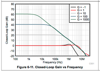
    Yes (21V/us) is what I used, but I also checked figure 6-11 from the data sheet. To me that shows it should work??? Also see my calculations below to show how I got to my conclusions.


    What SR should I be using if it is not the one given in the data sheet?


    I will setup a test using a 5V and 10V step. Do I need to change the gain back to 1 or is the gain of 10 ok for this test, since it will saturate the output with that large of an input anyway?


    Looking at the data sheet figures, the info given in the data sheet specifications and my calculations what am I missing?

    This will be a great learning experience for me since I obviously am missing some fundamental point in this simple design!


    Thanks guys for all your help with this!


    See my calculations and datasheet figure below.

    TI Analog Engineer’s Circuit Cookbook: Amplifiers (Second Edition)

    SBOA270A-February 2018-Revised January 2019

    https://www.ti.com/seclit/eb/slyy137a/slyy137a.pdf?ts=1621612875839&ref_url=https%253A%252F%252Flogin.ti.com%252F


    Inverting amplifier circuit Page 9


    My Design Goals

    Input

    ViMin= -0.5V

    ViMax= 0.5V

    Output

    VoMin= -5V

    VoMax= +5V

    Freq.

    50kHz

    Supply

    Vcc= 15V

    Vee= -15V

    My Implementation

    R1=1K

    R2=10k

    Gain = -10

    0.1 uf decupling caps on each supply pin to ground

    Output load is a X10 scope probe.

    +/- 15V linear supply


    Inverting amplifier circuit

    Step 4

    Calculate the small signal circuit bandwidth to ensure it meets the 50kHz requirement. Be sure to use the noise gain, or non-inverting gain, of the circuit.

    NG= 1+R2/R1 = 11

    GBP of the OPA991 = 4.5MHZ

    BW = 4.5MHZ/11 = 409kHz

    409kHz is well above the 50kHz needed


    Inverting amplifier circuit

    Step 5

    Calculate the minimum slew rate required to minimize slew-induced distortion.

    SR of the OPA991 is 21V/uS

    SR > 2 x Pi x f x Vp

    SR > 2 x 3.1415 x 50kHz x 5V = 1570kV/S = 1.5V/uS

    21V/uS > 1.5V/uS

    1.5V/uS is much lower than the 21V/uS of the OPA9901

    OPA991 data sheet info

    • Rail-to-rail input and output
    • Wide bandwidth: 4.5 MHz GBW
    • High slew rate: 21 V/μs
    • High capacitive load drive: 1 nF
    • Wide supply: ±1.35 V to ±20 V, 2.7 V to 40 V
    • High output current (±75 mA)

    Figure 6-11

    A gain of 10 is a closed-loop gain of 20dB. The graph below shows that 50kHz is well within range?

  • Hi Lidong,

    The 21V/us is the slew rate with slew boost turned on. This requires a large input signal. The natural slew rate of the device is significantly less than 21V/us which is why you are seeing a very slow response. The videos in TI Precision Labs on Slew Rate show the output response changes from a small signal to large signal as the input amplitude increases. I highly recommend watching the videos.

    If you test with a larger input signal, you should see close to the 21V/us slew rate datasheet specification.

    I recommend testing with a 10V step input. You will need to decrease the gain of the circuit so that the 10V step does not saturate the output.

    Thank you,

    Tim Claycomb

  • Hi Tim,

    I did run the input voltage up and did finally see the 21V/us. But that to me is like using the op-amp as a comparator? Where in the data sheet does it specify this very slow SR response for normal use?

    I made a costly mistake with this part and want to understand where in the data sheet I should have looked to see this slow SR response?  Don’t want to make this same mistake in the future!

    Thanks, I have reviewed the videos and they were very informative but did not answer this question?

    There is no warning or anything implying in the data sheet, best I can see, that the specified SR of 21V/us is only for a very specific input range, and if you do not meet this input range the SR is going to be a very slow SR of  XX V/us? See section 7.1 Overview in the data sheet. How would I design for this if it is not specified? What or where should I be looking in the data sheet to see this?

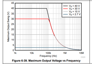
     Also can you explain why figure 6-11 and 6-39 shows that it should work at a gain of 10 and 15 volt supplies?  What SR is that figure using?

    I do appreciate all your help with this!

    After some 40+ years of designing am still learning! And that’s a good thing!

    If you were going to specify a part, what part would you go with?

    Low cost if possibleBlush

    Thanks again!

  • Hi Lidong,

    I think, when a OPAmp has "slew boost stage" then there's something unusual going on. And you shoudn't be surprised, if this OPAmp behaves strange or weird.

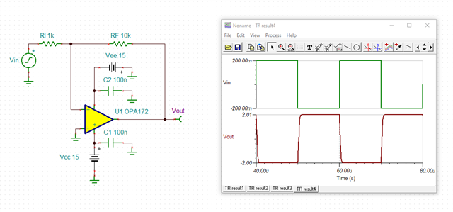
    I would choose an OPAmp without such a "slew boost" stage. I would give the TLV172 a try:

    50kHz sine:

    And 200kHz sine:

    lidong_opa172.TSC

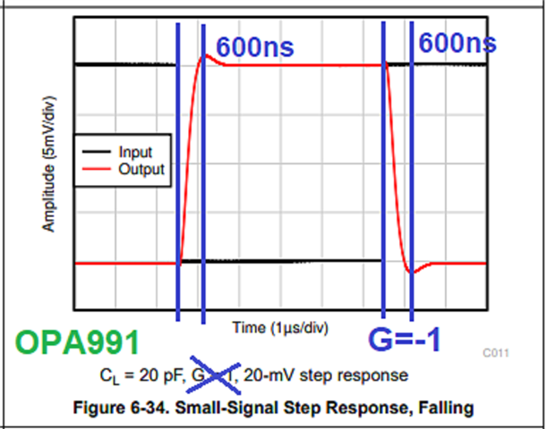
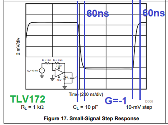
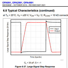
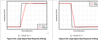
    And don't overlook the small-signal step responses. The OPA991 doesn't look very fast at all. Note how much faster the OPA172 is Relaxed

    Kai

  • After some 40+ years of designing am still learning! And that’s a good thing!

    Yes, but the datasheet should have been much clearer in this point Frowning2

    Kai

  • Hi Lidong,

    All amplifiers will see a reduced slew rate a small input amplitudes. This is because slew rate is a large signal behavior. It is not uncommon to require a few volt input to see the full slew rate of the device, especially if slew boost is used in the device. The OPA2991 is a little unique, in that it requires a little more input amplitude to turn on the full slew boost than most devices.

    There is nothing in the datasheet that mentions this behavior.

    What slew rate do you need for your design? The OPA2990 may work.

    Thank you,

    Tim Claycomb

  • Hi guys,

    It is just a little bit frustrating and a little costly but hey, live and learn.

    I will give the TLV172 and the OPA2990 a try and see where that gets me?

    Kai,

     I see where you used TINA-TI to show the LTV172 should work, but I also used TINA-TI for the OPA991 and it also showed it should work? I guess I am not so sure of the fidelity of these models anymore?

    You say “The OPA991 doesn’t look very fast at all”? Where on the data sheet are you seeing this? That is one of my questions. What should I be looking at to keep this from tripping me up in the future?

    The other question is how should I interpret figure 6-11 and 6-39 in the opa991 data sheet? Are those based on small signal or large signal? I would still like to know what the small signal slew rate is, if possible? Can it be calculated off of the data sheet somewhere?

    Tim,

    I just need the slew rate to pass this signal with minimal distortion. Per the step 5 calculations it looks like it needs to be over 1.5V/us if I did that right?

    All,

    Thanks for putting up with my questions! TI may want to adjust the data sheet to make this a little more clear in the future? It may help someone else? Specifying the small signal slew rate would be a great start, and when the boost turns on? Also the TINA-TI model could be updated to include the proper operation of this boost circuit functionality since it is somewhat unusual and I guess not common?

    I do really appreciate all your effort and help on this! I have learned a lot.

    I will try and get some samples of these parts through the TI Sample request program. I guess I will see how well that works?

    Again thanks for everything!

  • Hi Lidong,

    when comparing the small signal step responses, the OPA991 doesn't appear to be very fast:

    Kai

  • Hi Lidong,

    If a 1.5V/us slew rate is all that is needed then the OPA990 should work. However, please understand that there is a difference between small signal and large signal.

    Small signal rise times are dependent on the bandwidth of the device. Since the TLV172 has a higher bandwidth than the OPA991, then the small signal rise time will faster.

  • Hey guys,

    Thanks for your response!

    Kai,

    The attached figures helped a lot. From those figures I see the small signal slew rate for the OPA991 is

    0.02V/0.6us =0.03V/us that’s pretty slow.

    Per the figure for the TLV172 it has a small signal slew rate of

    .01V/.06us = 0.166V/us

    To me, based on the other calculation where 1.5V/us minimum was needed, this part would still not work?  Am I just out in left field? Nothing seems to add up to me?

    Tim,

    For the OPA2990 the small signal slew rate calculated off the data sheet figure is

    0.02V/0.5us = 0.04V/us which is smaller than the 1.5V/us needed???

    Oh, also TI declined my sample request!

    Thanks again!

  • Hi Lidong,

    when considering the small step response one should not think in terms of slew rate but rise time. And the figures I prepared for you demonstrate that the TLV172 is way faster than the OPA991. So there's a good chance that the TLV172 can do the job for you.

    Lidong,

    when using an OPAmp the number of applications is infinite. The datasheet cannot cover all these infinite applications but tries to give enough information for you to find out if the chosen OPAmp is a proper one for you or not. The same is true for the TINA-TI simulation. It cannot cover the full performance of an OPAmp, and it might even do a mistake when modelling the actual slew rate of OPA991.

    And because of all this, at the end only a test circuit built-up by yourself can show what's really going on and if the chosen OPAmp is satisfying your needs or not.

    I do have exactly the same problems when I myself am developping a new circuit. Many of the chips I take do not finally keep what the datasheet promises. But that's no ill will of the manufacturer of OPAmp but real life Relaxed

    There's no shortcut for a thorough development, unless the circuit is really really simple. And believe me, the development phase can be a stony stony road...

    Kai

  • Hi Lidong,

    As Kai mentioned, there is a difference between slew rate and rise time. A small signal does not go into slew limitation because slew rate is a large signal behavior. Instead, the small signal rise time is dependent on the bandwidth. You can calculate the rise time of small signals as 0.35/BW where BW is the closed loop bandwidth of the device.

    Thank you,

    Tim Claycomb

  • pretty much all of the high speed parts are slew boosted with a clean transition from small signal to large signal, it seems this OPA991 has more of a deadband than most slew boosted devices, also, your rise time estimate is old academic single pole response - which few parts have, 

    For a much more detailed linear to to slew limited discussion, the latest effort I put into that is in these two articles. There is a part 2 link in the part 1, couple of new and interesting results in here, 

    https://www.edn.com/what-is-op-amp-slew-rate-in-a-slew-enhanced-world-part-1/

  • Taking this just a bit further, testing the OPA2991 release model in its inverting gain of 1 for a large signal +/-5V input 1nsec edge gives this, calculates out to about 12.5V/usec

    There is one other useful plot, this large signal span - if we attribute the breakpoints to slew rate, you can solve by that Fcuttoff*2pi*0.707*(Vpp/2) =slew rate. Doing that across the different plots gives about 7V/usec - I am guessing this is non-inverting - there is typically a lower slew rate non-inverting gain of 1 vs inverting gain of 1. Perhaps the 25V/usec was just an optimistic number, Incidentally, this plot is often a measured plot - if so one would think any slew boosting would be fully engaged, looks like it gets it up to about 7V/usec if I read this plot correctly. 

  • I don't know if you are following all this, and I understand if you're not, you have better things to do, but it seems like everyone responding agrees that the data sheet and simulation model does not properly represent the real part?
    Knowing all  this now, who would I talk to about returning the parts I procured from TI? Do you have a name of someone who would understand the discussion and can help with this?  If you don't, that's cool too!
    Really, Thanks again for all your help!
  • Hi Lidong,

    What spec is not meeting datasheet limits?

    You mentioned previously that after using a large input signal you were able to see the full slew rate stated in the datasheet, correct?

    As I mentioned previously, the device uses slew boost to get to the full slew rate limit and most devices with high slew rate use this technology. To fully turn on the slew boost, a large input signal is needed. Slew boost is dependent on the input differential signal. As the inputs get closer and closer together (as the output signal rises, as shown in your original scope shot) the slew rate will decrease and eventually turn off, decreasing the slew rate of the device.

    Thank you,

    Tim Claycomb

  • At minimum, there is fair amount of inconsistency in "measured" data that would support the 21V/usec number, this inverting gain of 1 plot calculates to about 4.5V/usec. This plot would not be activating any input stage slew boosting so the native slew rate appears to be <<21V/usec. 

    These large swing gain of 1 plots do seems to show about 24V/usec on the slower edge but can you really count on that? It seems there is non-inverting input slew boosting that also pumps slewing current into the high impedance node for output stage support? What if you ran at a gain of +10 with less input swing, what slew rate should you expect. Comparing to prior art, it seems a bit of stretch to call this part 21V/usec across a decent range of applications. 

  • Hi guys,

    Sorry to keep dragging this out!

    This discussion has been very helpful and I understand the benefits of building a prototype/ proof of concept. I saw the TI hype on the OPA991 part and jumped on it to soon? Should have tested a few Frowning2 My bad!

    I also understand that data sheets aren’t perfect. I have been doing this for many years but this one confused me.

    Michael,

    Thanks for jumping in and helping. The slew rate calculations came from the TI cookbook, and yes I think this deadband is the issue?

     I will take a look at your link, thanks!

    Optimistic is a good word for this.

    All,

    I have procured the TLV172 and when it arrives I will run the same test I did on the OPA991. I will let you know the results.

    Again, Tim, Kia and Michael,

    Thanks for all your help and support on this.

  • Hi All,

    I am having the exact same problem with slew rate with the OPA2991.  I measured it to be around 0.47 V/us.  I have access to a nice Audio Precision analyzer, so I thought I would show the results I have achieved and hopefully add some clarity to the issue.

    My circuit consists of an RC highpass filter that is buffered then passed to gain stages of +8 and -8 V/V.  The OPA2991 is supplied with 40 VDC.  When I first noticed the strange behavior, I removed some components to simplify my circuit to the following diagram.

    I ultimately need to drive a 2600pF capacitive load at +/- 40V at around 20 kHz with a 40VDC supply from a 5Vpp input signal with minimal power consumption, so the OPA2991 seemed perfect.  The transfer functions I observed from the above circuit diagram are neatly summarized in the plots below.  I supplied input signals of 0.5Vpp to 3.5Vpp in 0.5Vpp steps, and plotted the differential output of my circuit as a function of frequency.  In addition, I calculated the slew rate at the frequency where each trace begins to fail, and all seven came out to be close to 0.47 V/us.

    Note that a higher input amplitude caused the failure to happen at a lower frequency, which seems contrary to some of the information I have read in this thread.

    It is very clear to me that I am hitting a limitation of the OPA2990, and that limitation was not reflected in the datasheet or SPICE model.

    Due to space constraints in my application, I chose the XFQFN-10 package for my prototype, which limits my options for a drop-in replacement.  Can someone recommend a replacement opamp that would meet my needs, preferably in the XFQFN package?

    Thank you,

    Mike

  • Hey Mike, 

    Here is parametric table for your desired packaged of X2QFN for all operational amplifiers in TI: www.ti.com/.../products.html

    It looks for your supply range (40V) you are limited to OPA2991 (21V/uS), OPA2990 (4.5V/us). 

    I think you should not see the following:

    Note that a higher input amplitude caused the failure to happen at a lower frequency, which seems contrary to some of the information I have read in this thread.

    This makes me think that there might be something else going on with your design.

    In summary both the OPA2990 and OPA2991 have slew boost, which means that the larger slew rate is not triggered without a large enough input signal. 

    If you would like a deeper dive into your issue, please start a new thread. 

    All the best,
    Carolina

  • Hi Guys,

    My LVT172 part arrived, and bellow are my findings.

    The circuit is the simple textbook inverting amp I showed at the very beginning of this thread.

    Note: I dropped the power supply rails from +/- 15V to +/-10V but still well within the range needed.
    Setup: Inverting Amplifier, Gain of 10, +/-10V Power Supply Rails, Basic requirement: 500mV peak input at 50kHz Sine wave. Expected output is a 50kHz sinewave at 5Vpeak minimal distortion.


    OP-Amp

    Input Voltage Peak

    Frequency

    Output Result*

    Basic requirement met

    TI price in qty 1000

    OPA991

    200mV

    20kHz

    Good

    $0.384      SOT-23 | 5

    500mV

    20kHz

    Distorted

    500mV

    50kHz

    Distorted

    No

    LM7301

    200mV

    20kHz

    Good

    $0.844      SOT-23 | 5

    500mV

    20kHz

    Good

    500mV

    50kHz

    Good

    Yes

    200mV

    100kHz

    Good

    200mV

    200kHz

    Distorted

    500mV

    100kHz

    Distorted

    TLV172

    200mV

    20kHz

    Good

    $0.334      SOT-23 | 5

    500mV

    20kHz

    Good

    200mV

    50kHz

    Good

    500mV

    50kHz

    Good

    Yes

    200mV

    100kHz

    Good

    500mV

    100kHz

    Good

    200mV

    200kHz

    Good

    200mV

    500kHz

    Good

    500mV

    200kHz

    Distorted


    Summary:

    The OPA991 was the worst performer but was supposed to be a better part then the LM7301 per TI?

    The LM7301 worked as expected.

    The TLV172 worked very well and is the lowest price part!

    *Note: The output results were based on visual inspection of an oscilloscope output waveform image.


    Again, very disappointed in the so-called better part of the OPA991? I am sure there is some application that this part will work better than the LM7301? I just do not see it yet.

    My project will move on with the TLV172! Thanks for that recommendation, that really helped! As I have said before, I really do appreciate all the help, insight, and time everyone has added to this discussion.

    Thanks

  • Thank you Carolina. With respect to the statement of mine that you quoted, the higher amplitude did cause the problem to happen at a lower frequency, but that was simply because a higher frequency results in a higher required slew rate.  My increasing input amplitude still was insufficient to enable slew boost.

    I want to echo the other user that the slew rate presented for OPA2991 is incredibly misleading.  Nowhere in the datasheet does it indicate that the slew rate would ever be lower than 21 V/usec.  From this thread and my experimentation, I learned that in many cases the slew rate will be roughly 0.45 V/usec, nearly two orders of magnitude lower than advertised.  At a very minimum, the datasheet should discuss the effects AND LIMITATIONS of slew boost.  I understand that you may not be able to reliably predict the input voltage at which slew boost will turn on, but it is negligent and misleading to make no mention of it whatsoever.

    This process has been a difficult and expensive experience for me.  Given the lack of information presented on slew boost, the main thing I have learned is to stay away from TI parts with that feature.

    Regards,

    Mike

  • Hey Michael, I think that is a bit overgeneralizing. Many newer op amps use some form of slew boosting to get a higher FPBW without the standing current. The most recent precision FDA's like the THP210 have an input stage slew rate boost as well as the THS4561, THS4551, etc. . This is all rarely noted, but you can kind of see it in the FPBW at low quiescent current. The OPA991 seems to be a bit of an outlier. Every higher speed op amp supplier works hard at getting a clean slew boost in many of their new developments - and most are very successful. If you did not see it early, here I tried to tie linear to slew limited performance together, part of what comes out of this is how easy it is to see true slew rate running a derivative on the step response. Not sure why I didn't make that a standard plot years ago. 

    https://www.edn.com/what-is-op-amp-slew-rate-in-a-slew-enhanced-world-part-1/

  • Hi Lidong,

    I'm happy to hear that the TLV172 works well for you Relaxed

    Kai

  • Hi Michael Obara,

    I agree with you that the datasheet should be much clearer in that point.

    In your special case I would recommend not to use a part with so little supply current. A supply current of 500µA (which is one third of the supply current of the TLV172 !) and a rise and fall time of 600ns in the small-signal step response indicates that the OPA2991 isn't actually fast enough for your application.

    A capacitive load of 2600pF means an impedance of 3k at 20kHz and lots of load current in combination with a +/-40V output signal. This should allow you to take an OPAmp with a considerable higher supply current. And you will get rid of all problems associated with the manufacturer's pull-ups to save supply current.

    Kai

  • Thank you Kai.  This experience has been educational for me, especially with respect to small signal step response.  Based on these posts, I have reduced my supply requirement from 40V to 36V and will try the TLV2172.  I am hopeful it will work.  I'm just not looking forward to reworking my PCB to get an SOIC wired into an XFQFN footprint. Slight smile

    Regards,

    Mike

  • Hi Michael,

    and if the TLV2172 is still not fast enough, choose an even more rapid one Relaxed

    Kai