This thread has been locked.
If you have a related question, please click the "Ask a related question" button in the top right corner. The newly created question will be automatically linked to this question.
Hello dear Ti community.
I know decoupling thread was explained thousand times and there is some general rules that should be followed.
But I've got some other questions that might be important as well.
So, I will try to explain my design and why I really care about those.
My desing is builded around few opamps and analog muxes.
I will look like this :
1x OPA1604 (audio input stage) 3x paralleled OPA1622 which will drive load directly (headphones), and analog mux around OPA1604 for gain manipulation (powered from bipolar supply).
This is one channel only.
I've got rather good PSU builded around ultra low noise LDO's.
Most common technique is to place 100nF capacitor as close as possible to IC pins (with opamps that are hi current output it's often recommended to place a bulk capacitor to provide enough charge).
And I already made that, each opamp got it's own bulk capacitor (10uF) followed by 100nF capacitor + another smaller like 1000pF.
My PCB is 4 layer board, so I can use internal layer for power to avoid thin/long power trace with significant inductance, or I can use outer layer to route fat enough power traces.
So PCb could be handled well by me and it shouldn't be an issue here.
Question is:
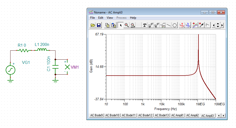
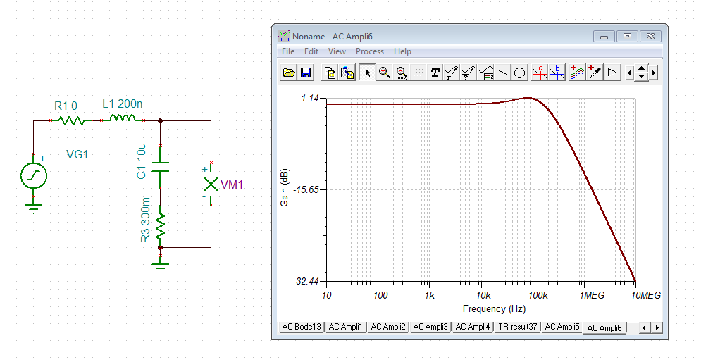
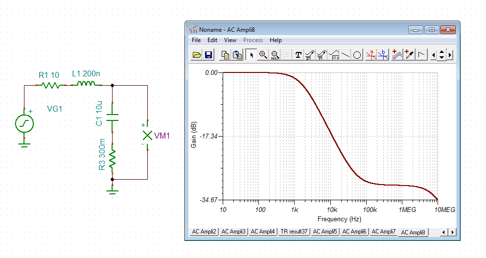
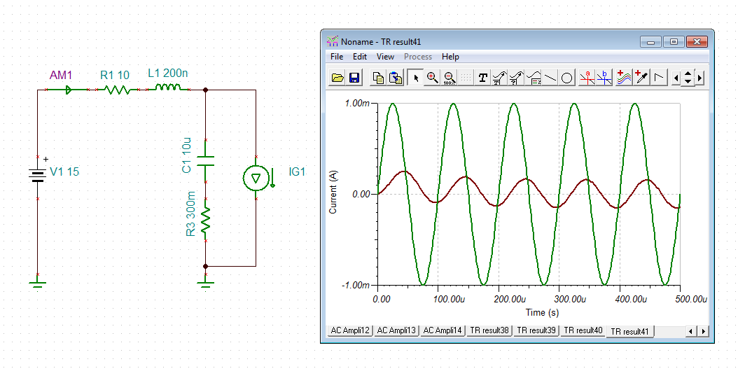
- should I isolate each opamp power supply from each other via ferrite bread (even if they are tends to work at higher freq) or resistor (I will affect dynamic range).
- or I should forget about it?
Should I include that kind of isolation? Imporant question is where should I care about it and when it's not required.
From theoretical point of view it's look promising, because it will improve opamp PSRR and it will make also make power supply cleaner, because there will be no "coupling contamination" that could harm other opamps.
I thinkg this is important because my output stage is AB class amplifier, that draw only half rectified current.
I also heard that placing multiple small value capacitors (like 100nF) for each power supply IC pins could resonate if connected to same power plane.
To avoid this I will need to add some damping.
So I'm looking for some more extended explaination of my post, because I'm aware about some things but I assume that it's still not enough.
Mateusz,
Decoupling is used to make voltage more consistent. The amount needed is based current requirement that exceeds the ability of the traces (inductance and resistance) to get the current form the next capacitor. Adding separation between between caps (like beads) reduces spreading of noise for one place to another. Every bit helps but there will be a diminishing return as you add more.
I will transfer post to another team so you can get an additional answer. None of the integrated circuits mentioned were in my group.
Hi Ron.
But adding some isolation via resistor or bread (which is often recommended for an MCU or hi speed OPA etc.) will make a tight local loop, so noise will stay there and will not flow over whole power supply line.
Am I right?
I'm still interested about theory when to use that isolation and maybe someone will be able to provide some information about it.
Hi Mateusz,
the following explanations are very simplified but are good enough to show the sticking points.
Assume you have a perfect power supply with presents 0R source impedance even at the highest frequencies. Further assume that you have an OPAmp circuit which is located about about 20cm away from the power supply. You take a 5mm wide copper trace for the supply line and have a continuous ground plane. You plan to decouple the OPAmp with a 100nF X7R. Everything looks fine but what you have forgotten is the inductance of copper trace of supply line. 20cm long copper trace gives about 200nH. In combination with the 100nF a resonance can be formed at arround 1MHz:
Now assume that you use a decoupling cap which has some ESR, like a 10µ tantal. Then the resonance almost disappears:
And if you finally add some series resistance the resonance can be furtherly suppressed:
One of the advantages of such a 1th/2th order low pass in the supply line is, that the OPAmp no longer draws all the supply current along the 5mm wide copper trace. At high frequencies most of the supply current is drawn from the decoupling capacitor and only a fraction of the supply current is drawn from the power supply being 20cm away. In the following a supply current of 1mA/10kHz sine is simulated:
By chosing the right decoupling capacitances this performance can be furtherly improved.
But you have to be careful, because the supply current of an OPAmp caused by the load is not necessarily of sine shape. This is only true for small load currents when the output stage is still running in class A mode. For higher load currents the output goes into class AB mode and the supply currents become distorted. But in the most cases this is not so much of a problem, because modern OPAmps can show a very good PSRR which suppresses this source of distortion. The pros of this methode must be carefully weighed against the cons and is part of the development.
Kai
Hi Mateusz,
when you discuss the stability of an OPAmp, it's not the signal band of interest (which is the audio band in your case) which counts but the unity gain bandwidth of OPAmp. Even if you amplify only DC voltages, if you do it with a HF-OPamp, this automatically turns your circuit into a HF-application. So, whenever you use a HF-OPAmp you must treat it like a HF-design.
I have learned that even the least amount of isolation is so helpful in increasing stability, that I always use it. In mixed analog digital applications I use for all involved chips power supply filters, even for the digital chips. It's the only way to keep the noisy supply currents within the local decoupling loops and to prevent the ground return currents from flowing back to the voltage regulators and contaminating the whole signal ground wiring. Have a look at my last simulation: It shows that the amount of supply current which flows through R1 (AM1) is only a fraction of the supply current drawn by the OPAmp. But remember, the current AM1 is the same current which flows across the signal ground back to the regulator, called the "ground return current". By this, the power supply filtering minimizes the current "traffic" on signal ground and helps to keep signal ground quiet and free from noise.
Keeping the signal ground as noise free as possible is the most crucial point in an ultra low distortion audio application. This cannot be said too often. Because of this I avoid supply planes and use instead multiple ground planes. As I use RC-filters in the supply lines of OPAmps anyway, I don't need the ultra low impedance the supply plane is offering. But this is my personal taste. I know that other designers are thinking differently.
What supply filtering is good for your circuit cannot by said by a rule of thumb. It depends on your actual circuit. In any case you must follow the decoupling recommendations given by the datasheet. Usually a low ESR 100nF/X7R is recommended. Then you can put a cap with much higher capacitance and much higher ESR in parallel to this cap. Put them close together and place them as close as possible to the supply pins of OPAmp. The filter resistor should also be located near the decoupling caps but need not to sit directly at the supply pins of chip. The value of supply filter resistor mainly depends on the load current.
It's not wise to place an armada of decoupling caps at the supply pins of OPAmp. Too many decoupling caps can hinder each other. If the 100nF caps cannot be placed directly at the supply pins, the armada is worthless. Also, several low ESR caps can show nasty resonances when being paralleled, eroding the decoupling performance for certain frequency bands.
Kai
Hello Kai.
Sorry for my late reply, but your help is very apprieciated :)
That kind of replies are what I was looking for quite some time.
Taking advantage of the opportunity I've got another question.
Let's imagine a typical power supply with center-tapped winding which is followed then by diodes and then a bulk capacitor.
Question is how much ripple is allowable?
I know that capacitor calculation will be load dependent.
I found a equation :
C = 0.7 * I /(ΔV * F)
I"m also aware of that ripple voltage should be "added" to drop-out voltage.
So if my LDO will work perfectly fine when VIN is 1V higher than VOUT then I should add riple to that 1V to achieve good performance.
And here we go again, I also know that ripple will be capacitance dependent, so if I pick bigger capacitor then I will get less ripple.
But this is somethimes a waste of money and space.
My question is rather simple, how much ripple is allowable (in your option) especially when we're going to feed this "raw" supply in a front of hi performance LDO.
Or maybe that thread is more expanded and I also should consider ripple and a regulator performance to find a best price/performance point?
If there will be some diffrences between examples then let's assume typical circuit with LM317/LM78xx and something better like TPS7A4701 (both hi current).
Another question might be kinda newbie.
But most audio eq. got very big transformers inside (oversided), question is how to pick a proper power ratio?
Let's assume that I will spend all of LM317 current and it will be set to 15-18V.
Transformator windings will be picked to mantain a proper voltage regulator and to not overheat regulator (high VIN compared to VOUT).
Hi Mateusz,
this depends on so many factors that there is no simple answer. What you also must take into consideration is mains voltage fluctuations of at least +/-10%. So, your headroom of the regulator's input voltage must be much wider: 1V for the drop out voltage, 1...3V for the ripple voltage and 2...3V for mains voltage fluctuations.
How you proceed mainly depends on the maximum supply current of your application and what you can spend for the cooling. In many of our products we generate a somewhat higher supply voltage at the storage cap behind the bridge rectifier and use a DC/DC switcher as pre-regulator to create a rather stable voltage for the LDO. This two stage design has many advantages: The switcher has a much higher efficieny and needs much less cooling and the LDO provides a noise free supply voltage without having to deal with high differential input to output voltages. A design could have the following parameters: Generating 25V at the storage cap, using a LM2674 to generate 18.5V and finally taking a LM317/LM7815 for the fine regulation. Furthermore, placing a suited pi-filter between the LM2674 and the LDO.
But again, it depends on the maximum supply current of your application and on what you can spend for the cooling.
Kai
This is indeed very useful information.
I was never thinking about step down converter, but I'm aware that they're exist.
Your option is somehow similiar to placing SMPS like MeanWell IRM series.
Should I consider higher switching freq for a DC/DC converter?