Part Number: THS4631
Dear TI expert,
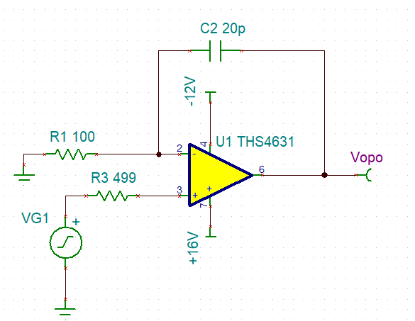
I design a PCB in which a THS4631-based integrator is used. The circuit is as Fig1. The power supply for 4631 is +16V and -12V, feedback capacitor C2 is 20pF, R1 is 100 ohms, which leads to high output voltage slopes.
Fig1
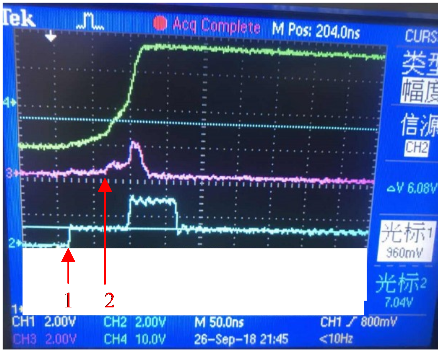
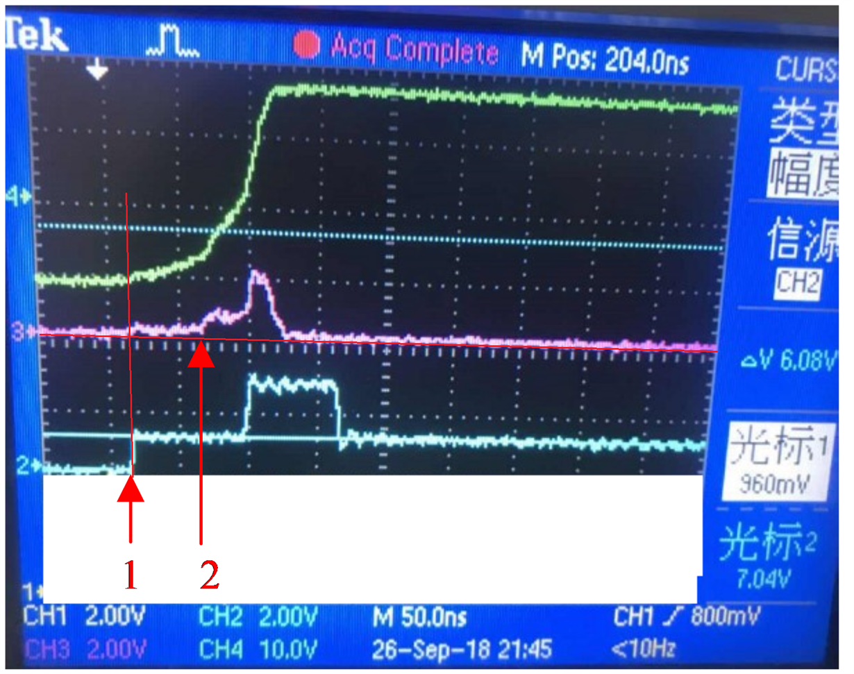
I step VG1 from -1V to +1. The waveform is as Fig2, where blue waveform is VG1, red one voltage at inverting node and green one is the output voltage Vout. Note that at time point 1, the VG1 steps to 1V, however, after about 60ns, the inverting and output node begins to act at time 2.
Fig2
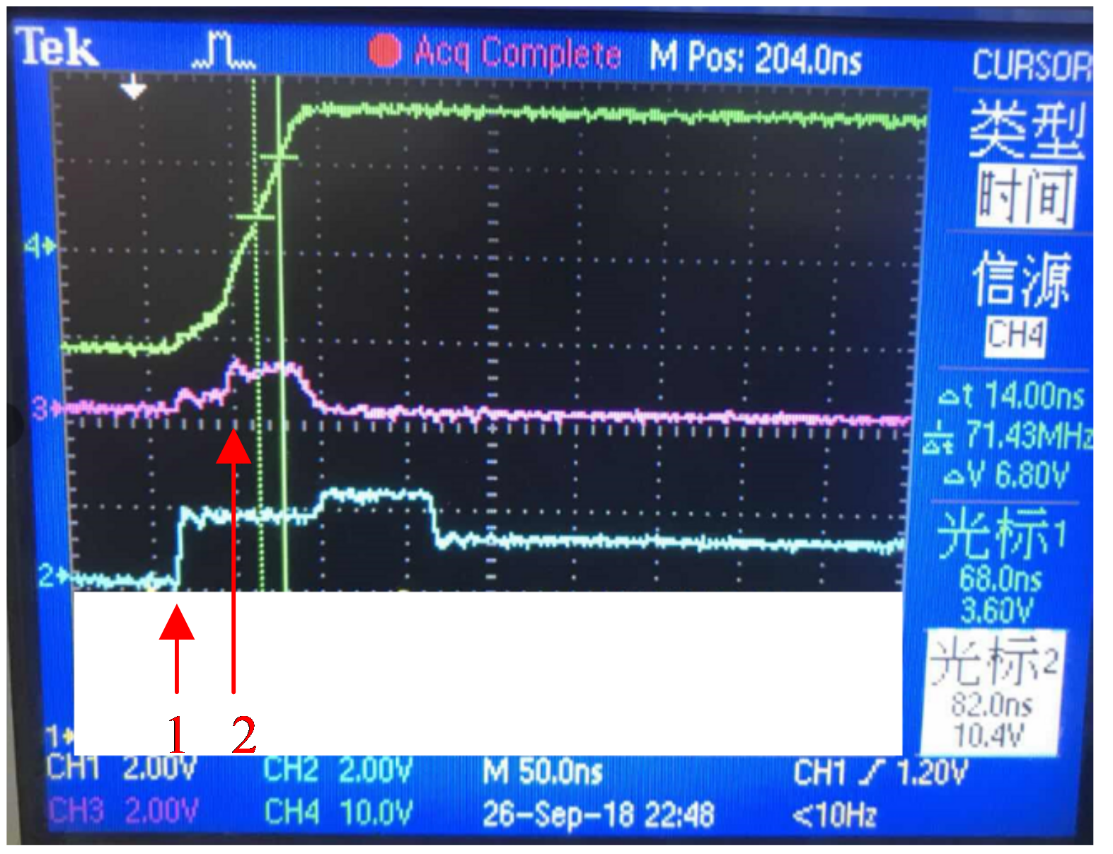
I then step VG1 from -1V to +1.5V, and the waveform is as Fig3. Note that the delay is reduced to about 40ns but is still there.
Fig3
I then try to change R1 in Fig1 to 499ohms, and VG1’s step to +5V. The experiment shows the delay is very small and negligible. The waveform is not given here.
I do the test in TINA and finds no such interval between time 1 and 2 as observed in Fig2,3. In the simulation, - and output node voltage act very quickly.
In theory, when VG1 steps to 1V or 1.5V(large signal), given the inverting node is 0V, THS4631 should immediately rise at a slope of several hundred V/us.
I wonder what may lead to the delay.
If you need further detail about my PCB design of this part of integrator or other information, just inform me.
Best Regards
Yatao


