This thread has been locked.

If you have a related question, please click the "Ask a related question" button in the top right corner. The newly created question will be automatically linked to this question.

LM6171: How to keep the op amp off its saturation region?

Part Number: LM6171
Other Parts Discussed in Thread: THS4631

Hi TI expert,
My question is a follow-up of the one in thread e2e.ti.com/.../732403. In that thread, kai klaas69 tells me the reason why the op amp –based integrator has an obvious response delay to its input’s step is due to the op amp’s desaturation.
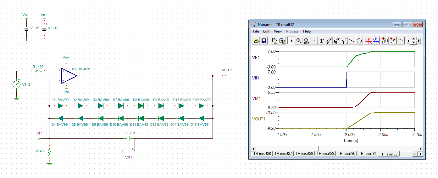
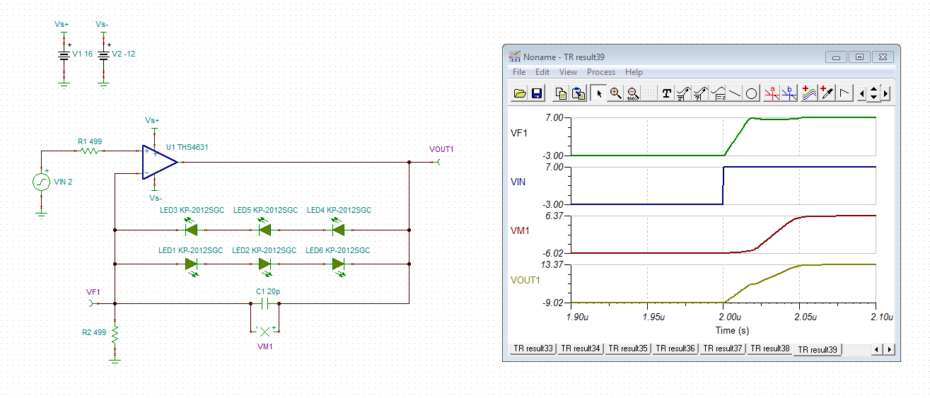
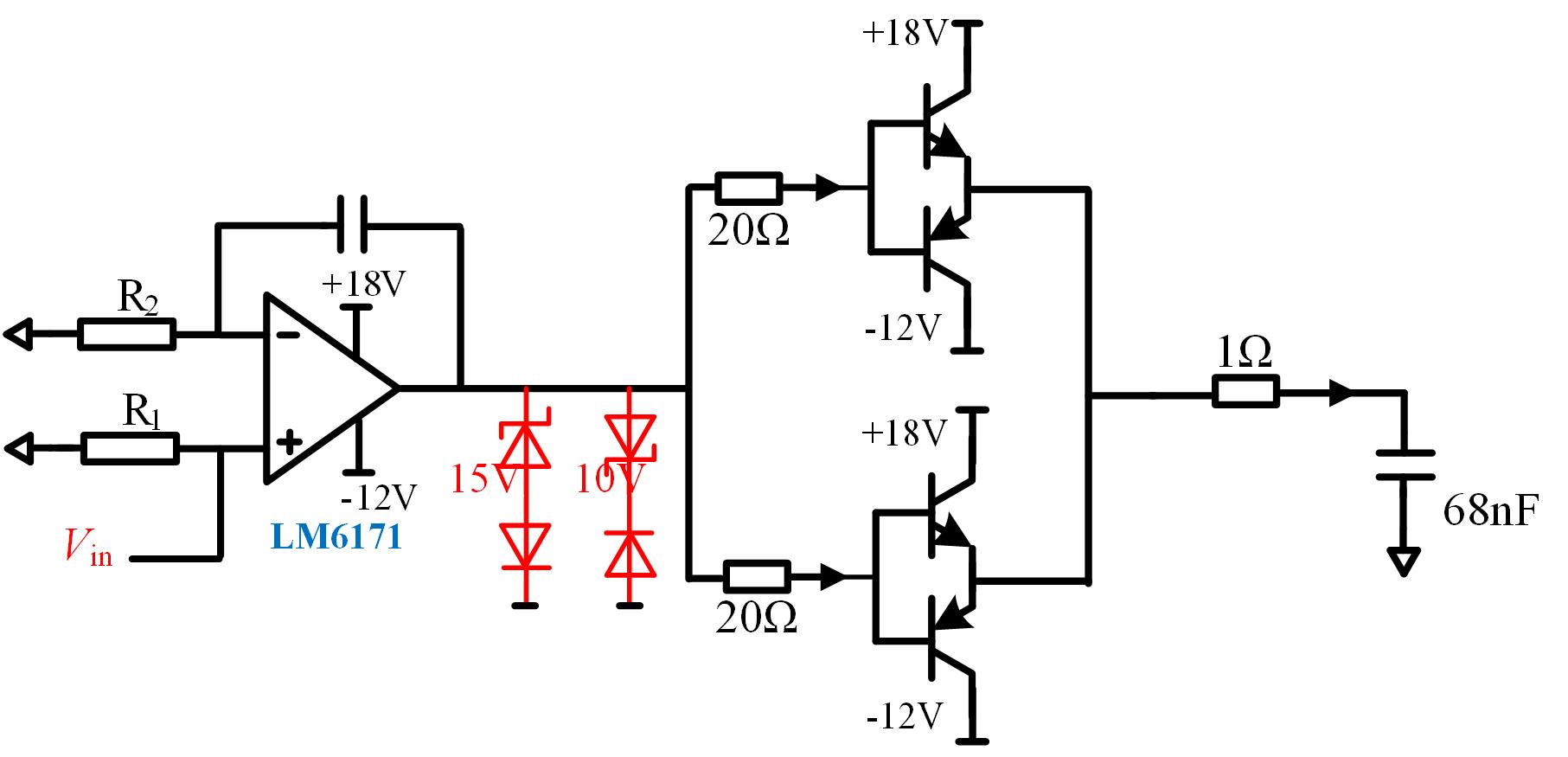
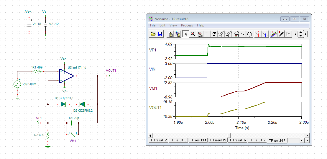
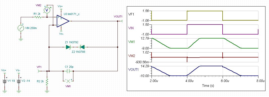
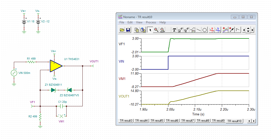
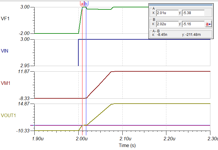
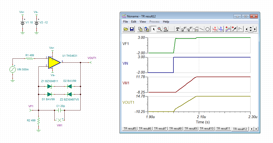
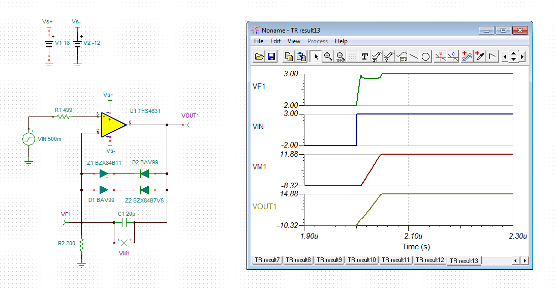
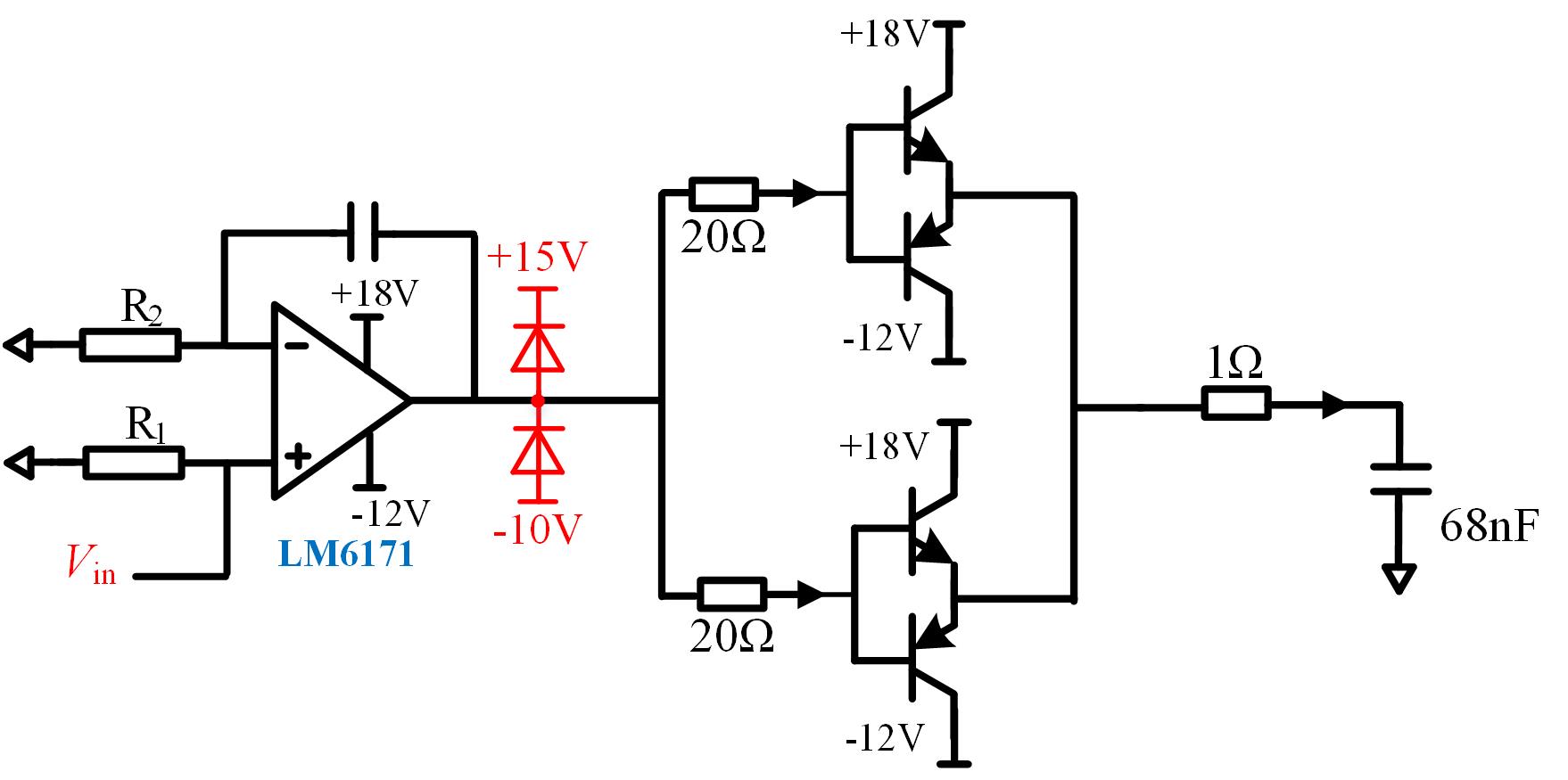
In my application, I want to produce a voltage in the range of -10V to +15V in the RC load. Then, to solve the saturation issue, can I supply the op amp with -12V and +18V and put two diodes at the op amp’s output node to clamp the output within -10V and +15V? The schematic is as below. I wonder is this method effective? And any other ways to keep op amp off saturation region?(You see, this method isn’t quite convenient, taking the other supplies into account.)

Regards 

Yatao

  • Hi Yatao,

    I don't think that this will work, because this would mean to short circuit the output to the rails.

    One method to prevent saturation is to clamp within the feedback loop. In your case a lot of diodes would be needed, which does not look very realistic:

    yatao1.TSC

    Another way is to use low capacitance LEDs:

    yatao2.TSC

    Kai

  • Hi Kai,
    Somehow I didn't receive the notification email, so I thought you haven't replied me. Sorry for the delay.
    As to your second suggestion, different from a normal integrator whose '-' terminal voltage stabilizes to 0 Volt, the '-' terminal voltage is very large when stable, bringing some trouble to my control goal.
    I wonder if you are sure my proposal won't work. In my opinion, if LM6171's output stage is comprised of push-pull BJTs, then when I use the clamping diodes, their BJTs's Vce are about 2V or 3V, causing them to work in amplification region. This link http://www.analogzoo.com/2014/12/op-amp-recovery-and-slew-rates/, gives an example of clamping op amp's output with a diode. If this is true, then I think this is worth a try.

    I come up with another circuit like the one below. 15V and 10V TVS are used and each of them are in series with a diode to avoid the TVS cause short circuit.

    If you're sure that these won't work, are there other convenient alternatives?(Is my application requirement very unique?)

    Regars
    Yatao

  • Hi Yatao,

    Overdrive recovery is caused when the amplifier cannot maintain a virtual short between the inputs, and a voltage charges the capacitance between the inputs. This must discharge before the amplifier will return to normal operation. The circuit in this article does not prevent overdrive recovery, it just lowers that voltage and therefore slightly decreases the recovery time. It still short circuits the output, which is not good design. A clamping diode in the feedback parallel to the capacitor is preferable. You could use 2 series, in the opposite direction, zener diodes if you want to minimize components.

    Best regards,

    Sean
  • Hi Sean,

    Thanks to you and Kai, and I decide to use 2 Zener diodes to prevent op amp’s saturation.

    Just to confirm, I plan my configuration as the schematic below, with one diode’s Zener voltage 12V and the other 8V. Meanwhile, the input voltage Vin has magnitude of +3V and -2V. Then, as the schematic shows, this integrator’s output voltage will be within -10V and +15V and the op amp will operate away from the saturation region. Am I right?

    PS: I will choose low-capacitance zener diode. But I wonder if TVS diode is more suitable, considering TVS’s switching time is less than 1 picosecond?

    Regards

    Yatao

  • Hi Yateo,

    clamping the output of LM6171 to signal ground by the help of zener diodes or to a bias voltage by the help of small signal diodes causes an output current of more than 80mA! Driving the output into the short circuit current limit of OPAmp also causes a sort of saturation and I don't think that doing this is a good idea.

    Using zener diodes in the feedback path sounds to be a good idea, but unfortunately the junction capacitance of a standard small current zener diode is rather high, which will affect the integration capacitance. Also, the junction capacitance is not linear with the applied voltage. Because of this I suggested the series circuit of many BAV99. The effective capacitance of such a series circuit is much smaller than your integration capacitance and doesn't play any role. Even a series circuit of LEDs can be useful. So, if you try zener diodes look for variants with very low junction capacitance.

    Using a TVS might not be a good idea. They usually have a very short turn-on time, but suffer from a long turn-off time. Look for a TVS with little junction capacitance and short reverse recovery time.

    Kai

  • Hi Yatao,

    I have made a simulation with your proposed low capacitance zener diodes:

    yatao3.TSC

    Kai

  • Hi Kai
    I'm very thankful for your kindness to help me.
    In fact, I haven't decided to use your two proposals, just because that my application requires +15V and -10V, and errors of several hundreds of mV is permitted. However, your proposal gives -9V and 13.38V, which is just too far away.
    The two diodes I proposed are limitted by 100mW(maximum power rate) and can not be used here. I tried hard and find Panasonic's(Japan) low capacitance zener diode industrial.panasonic.com/.../DD3X062J0L_E.pdf, which can be connected to form the right zener voltage.
    I really don't want to bother you. But can you please tell me how to use regular diode(BAV99 and so on) to create +15V and -10V. I'm very careful with the design because if the PCB I make fails to work, then I'll need to modify it and make a new version PCB, which takes too long time.

    Regards
    Yatao

  • Hi Yatao,

    Since the clamping will be logarithmic, like a diode curve, It depends on your max input voltage step. Higher input voltage= fewer diodes (lower clamp voltage at higher current). To make these clamps, multiple series diodes will give you lower parasitic capacitance than two Zener diodes, as Kai noted. They do not all even have to be the same diode type. You can combine types to get the desired clamp voltage for the max input voltage and integration gain resistor. You might include one that is low leakage in reverse bias, to lower the "jump" that clamp leakage current will induce at the output when the integration switches polarity. The tradeoff between either lowering parasitic capacitance and increasing clamp accuracy or diode count is up to you. I like Kai's LED clamp, which is a good median with the added benefit of lighting up to show you when it is clamping. I simulated a -1V to +1.5V input step with a 13V and 9.1V Zener.

    Best regards,

    Sean

     Ling.TSC

  • Hi Yatao,

    I would give this scheme a try:

    I think the BZX84B11 and BZX84B7V5 can be used here. Please note that I have taken the THS4631 again.

    Kai

  • Hi Kai,

    You are so nice.

    Just now, I was about to use several LEDs in series to clamp the output. Then you give new hope to achieve my goal with fewer diodes.

    I’ve tried TINA simulation with BZX84B11 and BZX84B7V5 with lower integration resistance, 200ohms. The result is as Fig1. I’d give some analysis here.

    Fig1

    As you can see, at the input step, the output rises sharply due to the input difference and the inverting node rises at the same speed since BZX84B7V5’s clamping. Then at cursor a, input difference reaches zero. After cursor a, the integration resistor’s current begins to discharge BZX84B7V5 and the process is the short interval between cursor a and b, during which VM1 and Vout rises with same low speed. At cursor b, BZX84B7V5 no longer serves as a 8V dc supply but a voltage-dependent capacitor. Then this integrator comes back to the behavior of a normal one, with no zener diodes. If the plateau process between cursors is seen as the desaturation of BZX84B7V5, then we are actually using BZX84B7V5’s saturation to replace op amp’s saturation. Luckily, the former one features a much smaller recovery time, approximately 9ns. Beside, when input drops to -2V, the plateau for the decreasing process lasts 20ns.

    You emphasize the use of THS4631, which leads me to try LM6171. The simulation result with 200ohms integration resistance is as Fig2.Its performance is slightly worse than THS4631. For example, inverting node’s voltage suffers from an obvious overshoot.

    By the way, I’ve always doubted that, to what extent can we trust TINA’s result. Because as you see, the integrator’s desaturation delay, which is obvious in my experiment, never appears in the simulation results.

    Best regards

    Yatao

  • Hi Yatao,

    your analysis is correct. Zener diodes are not optimal for fast switchings. But when using a BAV99 instead of the forward biased zener diode, you can improve the performance a bit:

    And when additionally decreasing the integrating resistance, the performance can be furtherly optimized:

    yatao5.TSC

    Kai

  • Hi Kai,
    You already have given me a lot of choices and I'll try to pick one from them.
    I've learned a lot from you guys, what can I do to express my thanks to you?

    Regards
    Yatao