This thread has been locked.

If you have a related question, please click the "Ask a related question" button in the top right corner. The newly created question will be automatically linked to this question.

Input supply to OPA548

Other Parts Discussed in Thread: OPA548, TINA-TI, OPA549, OPA547

Hello,

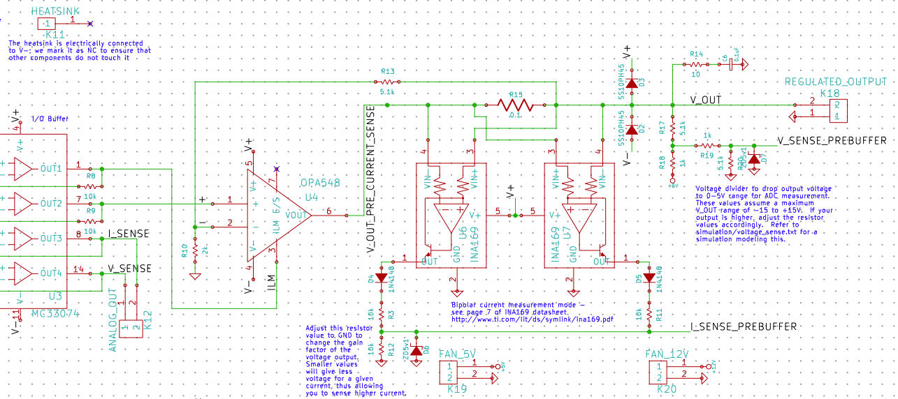
I am designing a benchtop power supply using OPA548 as the core regulator.  You can view details of my plan (if desired) at:  

My question is whether I need to regulate the VS input supply (+ and -) prior to feeding it into the OPA548?  My plan was to feed the OPA directly from the rectified A/C (filtered by two 22000uF caps).  In simulations, the output of the rectifier has very low ripple levels even under heavy load, but there is some voltage drop when drawing a lot of current.  My concern is that, since the current limit is referenced to V-, that even slight fluctuations on V- would cause problems.

If pre-regulation is needed, I would put a couple of LM7x15 with power transistors on the input rails to keep VS at a constant regulated state.  This option is just a bit annoying as it would increase board size substantially, due to the space needed for power transistors and the accompanying heat sinks.

Thank you very much for your suggestions!

Cheers

  • As a bit of a followup here, I have gone through the data sheet and have been unable to find the answer to this.  I have a suspicion that it may be related to the PSSR graph, but despite researching this I have been unable to understand what is being shown.  (I am not an engineer, unfortunately...)

    Thanks again in advance for your help!

    Cheers

  • There are several concerns with your design:

    1) You have many loops for current or voltage feedback that may or may not be stable, especially as you connect reactive loads.

    Here is a link to an op amp stability tutorial you may find useful:

    http://e2e.ti.com/support/amplifiers/precision_amplifiers/w/design_notes/2645.solving-op-amp-stability-issues.aspx

    2) You can simulate power supply ripple and its effects n your op amp circuit using the free TINA-TI simulator:

    http://www.ti.com/tool/tina-ti

  • Deciphering Op Amp DS_revA.ppt

    Attached is an op amp spec presentation that can help you understand effects of PSRR and how they will be seen on your output.

  • Stabilizing Inductive V to I Circuits.pptx

    If your Power Supply will ever drive inductive loads with current sense (constant current source configuration) you will have different op amp stability concerns as discussed in the attached presentation:

  • Hi Wyatt,

    Looking over your power supply circuit schematic it indicates that you plan to directly interconnect, pin-to-pin, two OPA547, OPA548, or OPA549 power op-amps. That is not something we recommend. Functions, such as the I-lim, senses the current in its associated output stage and is not intended to be tied to other I-lim pins. Even more of an issue is tying the output pins directly together. The differences in input offset voltages between amplifiers can result in the two amplifiers sinking and sourcing current between each other, which adds to their dissipation. That is why ballast resistors are used in the parallel-connected op-amp circuits as shown on OPA548 data sheet page 16, Figure 21. They limit the current that can flow between the two amplifiers and decrease the unintended dissipation. They will add a little to the phase margin which may help when driving a capacitive load.

    You can't know for certain what sort of load will be connected to the output of your power supply. There may be certain reactive loads that would cause the amplifier to become unstable. That would need to be assessed.

    The OPA547/ OPA548 has good power supply rejection (PSRR) at 100 to 120 Hz. (see data sheet pg. 5). The +PSRR is about 95 dB (17.8 uV/V), and the -PSRR is about 80 dB (100 uV/V). So in the case of the latter, the output offset will change 100 uV for each 1 V change in the negative supply voltage level.

    You really might want to consider tying in with an engineer and have them go over your design to make sure that it is sound and will do what you expect.

     Regards, Thomas

    PA - Linear Applications Engineering

  • Hi Thomas,

    Thanks for your comments!  Just to clarify, I am not going to put two 54x op amps in parallel; rather, the board design allows for populating exactly one of these.  The reason I am doing this is for board re-use, so that the low cost board manufacturing houses that provide 10 copies of the same design can be utilized better.  When looking at the schematics, you can completely ignore one or the other of the two op-amps in parallel; only one of them will be populated on a given board.

    Attached is a simplified version of the schematic, with the OPA549 removed.  This is closer to how a given channel of the power supply would look.

    Thanks again for your time, it is most appreciated!

    Cheers

  • Thank you very much for your responses, Tim. I will read over all the links you sent and see what I can come up with.

    Cheers