May I know which TI opams can run under gain 1?Because I want to reduce the voltage level down to fit the voltage range of THS1209 ADC. can opa2277 fit my requirement?
Many thanks.
This thread has been locked.
If you have a related question, please click the "Ask a related question" button in the top right corner. The newly created question will be automatically linked to this question.
Pretty much any op amp or FDA can act as an attenuator, Running non-inverting with an op amp, you simply put an R divider into the V+ input to get the attenuation and run the (unity gain stable) op amp at a gain of 1, running inverting op amp or FDA, you simply run it as an attenuator, there are of course several nuances to consider, some discussed here, You will occasionally see an article or app note claiming you cannot safely do this - those are misleading,
To zero in on your requirement, more application detail would be needed.
Hi 5111212,
Here are two options. As Michael indicated, near all op amp can attenuate the input signal in this manner.
If you use OPA277 or OPA2277, please watch out for common mode voltage requirements. If you provide us with your attenuation and op amp requirements, we can check out a circuit for you.
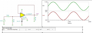
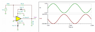
Best,
Raymond
Hi, Raymond
I plan to use OPA2277. The power is the dual supply +-12V and the signal level is +-12V, I want to get 1/8 gain.
Please let me know the setting of the attenuator based on OPA2277 and THS1209 can provide +2.5V reference .
Many thanks.
David.
I forget sth, THS4131 will be connected after OPA2277 to transfer single-end signals into differential-signals for feeding THS1209 ADC. The +2.5V reference from THS1209 will be connected to THS4131, so OPA2277 will need +2.5V common mode voltage. Please let me know the setting for above configuration.
Many thanks.
Hi 5111212 ,
The power is the dual supply +-12V and the signal level is +-12V, I want to get 1/8 gain.
Enclosed is a circuit that will meet the above requirements.

I have some questions. THS1209 is ADC with BW is 2MHz. But THS4131 is a high speed FDA with BW of 150MHz. I don't think that you will need 150MHz Op Amp to connect between OPA277 and THS1209 ADC (I think that THS1209 can do single-ended or differential input ADC mode).
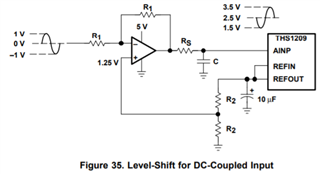
Are you using THS1209 in a differential mode? If so, you may use THP210 Op Amp to attenuate the input signal and interface directly to differential input of ADC.
Please let us know if this is what you have in mind.
Best,
Raymond
The other more reasonable FDA options would be the THS4561- in either case you could run them single 12V supply and level shift to the output Vocm set point, The THS4131 looks very low noise and it is, but once you include the R noise terms those dominate.
Yes, you are right. I am using THS1209 in differential mode. I will see if THP210 fit my need.
Many thanks.
David.
also, why don't you just use the FDA to do the attenuation and get rid of the first stage
Even on a single supply, a part like the THS4561 or THP210 will level shift their I/O pin swings into range with a +/-12 input - but you should confirm that with simulations, I tried to discuss some of this on page 33 of the THS4551 datasheet.
Hi David,
Here is an example of SE to FDA with attenuation.
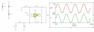
THP210 SE to DF Output 03172021.TSC
https://www.ti.com/lit/an/sloa099/sloa099.pdf
If you'd like to use THS4551 HS Op Amp, I can transfer you to the support team tomorrow.
Best,
Raymond
Hello Raymond and David,
Actually, the FDA attenuator is quite simple - if a bit confusing. It should work with any FDA, you just need to choose by desired speed and precision which to use. The design starts by targeting an output Vocm voltage and a +/-swing around that. Running single supply, if you keep the output in range (not clipping into the rails) the non-signal input side is a simple R divider to ground. Since the output feeding that is not going below ground, neither does the fed back input signal - staying in range, here is your sim file simplified to a 1/8 gain (you don't need that R to ground) showing just the output swings - this is taking +/-12V input to the 2.5V output centered swing using single 5V supply, I tried the THP210 here, it was not setting up the output Vocm correctly - I think the part would be fine, but the model was not so I went to the THS4561 model,
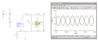
And then here are the two summing junction voltages - magically inside the supply voltages and not clipping, Since the differential voltage has to be zero, these are on top of each other.
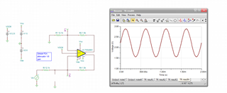
So you can actually do this function pretty easily with any FDA-This is because of that separate common model loop driving the input common mode voltage swing. . The design starts by setting.
1. desired output Vocm
2. desired +/-V on each side of that on the two outputs
3. that sets the attenuation
4. Then, going further what bandwidth do you want and then do you want any MFB filtering in the FDA stage - pretty easy to do
5. Once you have the RC values set around the part (including any RC into the ADC), check the phase margin
6 If the phase margin is poor, there a couple of easy ways to fix that.
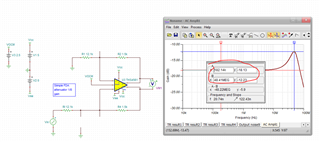
Here is the single 5V 1/8 attenuator design with the THS4561
I went on to look at the SSBW here, yes a little peaky - that is normal as most of these FDA's are nominally design and specified at a signal gain of 1, that is a noise gain of 2, here we have NG of 1.125 so yes, a little lower phase margin - this 6dB peaking implies a 29deg phase margin using Figure 2 in this article, this is all easy to fix, but would be better to get closer to end design and device.
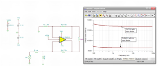
Incidentally, here is an output noise comparison between the two - lot of other things going into this, but using an input divider raises the noise gain giving more gain to the output for the FDA input voltage noise, If that can be avoided, as shown with the THS4561 ckt, normally lower noise can be delivered.
michal,
Many thanks for your great design. I will follow your idea.
I have one more question, should the output of mux36s16 connect the buffer before interfacing FDA?
Many thanks.
Probably since the MUX on resistance and capacitance will interact with both the signal path gain and noise gain balancing between the two sides.