This thread has been locked.

If you have a related question, please click the "Ask a related question" button in the top right corner. The newly created question will be automatically linked to this question.

AM437x DDR3 read issue

Other Parts Discussed in Thread: AM4377

Hi,

We use AM4377 processor in our custom project board and we face the problem of unsuccesful DDR3 initialization when uploading the GEL files. We modified the IDKAM437X DDR3 settings in AM43xx_EMIFconfig_HWlvl as we based the hardware part on IDKAM437X. The DDR3 used in different so there are a lot of changes to be done. Unfortunatelly, DDR3 reading test is not passed. We wrote our code for broader analysis and discovered that there is a pattern in those errors - every time we access the cell of the following address endings: 0x0 ; 0x1 ; 0x8 ; 0x9 we get the wrong value. For instance our test reults look like that:

CortexA9: GEL Output: Binary: Addr:0x80000000, Expected: 0xAAAAAAAA, Read: 0xAAAA0020
CortexA9: GEL Output: Binary: Addr:0x80000001, Expected: 0xAAAAAAAA, Read: 0xAAAADCEB
CortexA9: GEL Output: Binary: Addr:0x80000002, Expected: 0xAAAAAAAA, Read: 0xAAAAAAAA
CortexA9: GEL Output: Binary: Addr:0x80000003, Expected: 0xAAAAAAAA, Read: 0xAAAAAAAA
CortexA9: GEL Output: Binary: Addr:0x80000004, Expected: 0xAAAAAAAA, Read: 0xAAAAAAAA
CortexA9: GEL Output: Binary: Addr:0x80000005, Expected: 0xAAAAAAAA, Read: 0xAAAAAAAA
CortexA9: GEL Output: Binary: Addr:0x80000006, Expected: 0xAAAAAAAA, Read: 0xAAAAAAAA
CortexA9: GEL Output: Binary: Addr:0x80000007, Expected: 0xAAAAAAAA, Read: 0xAAAAAAAA
CortexA9: GEL Output: Binary: Addr:0x80000008, Expected: 0xAAAAAAAA, Read: 0xAAAA0000
CortexA9: GEL Output: Binary: Addr:0x80000009, Expected: 0xAAAAAAAA, Read: 0xAAAAFCFF
CortexA9: GEL Output: Binary: Addr:0x8000000A, Expected: 0xAAAAAAAA, Read: 0xAAAAAAAA
CortexA9: GEL Output: Binary: Addr:0x8000000B, Expected: 0xAAAAAAAA, Read: 0xAAAAAAAA
CortexA9: GEL Output: Binary: Addr:0x8000000C, Expected: 0xAAAAAAAA, Read: 0xAAAAAAAA
CortexA9: GEL Output: Binary: Addr:0x8000000D, Expected: 0xAAAAAAAA, Read: 0xAAAAAAAA
CortexA9: GEL Output: Binary: Addr:0x8000000E, Expected: 0xAAAAAAAA, Read: 0xAAAAAAAA

We have tried many different memory settings in the registers: CTRL_DDR_ADDRCTRL_IOCTRL, CTRL_DDR_ADDRCTRL_WDX_IOCTRL, CTRL_DDR_DATAX_IOCTRL, EMIF4D_DDR_PHY_CTRL_1, EMIF4D_SDRAM_CONFIG, EMIF4D_SDRAM_TIMING_X, EMIF4D_SDRAM_REFRESH_CTRL, EMIF4D_SDRAM_OUTPUT_IMPEDANCE_CALIBRATION_CONFIG according to the DDR memory datasheet.

We are out of ideas even after reading the TI tutorials about DDR configuration. Could you please advise us in which part of our configuration the error could be? - do we have to look deeply into DDR3 size (rows, columns, banks) or its timing? We are noobies in this subject so maybe there is someone more experienced in DDR3 programming who would like to advise us.

Thanks!

JJ

  • Hi,

    Is this a single board, or you see the same issue on multiple boards?
  • Hi Biser,
    Exactly the same response is observed in our 3 boards.
    Best,
    JJ
  • Can you post the DDR schematics?
  • Hi Biser,

    We followed the IDKAM437X board schematic - here there is the part of our with the DDR connections:

    Schematic DDR3.pdf

    Best,

    JJ

  • Yes, we filled the table and an application engineer of the memory manufacturer verified it.
  • Can you post the spreadsheet as you filled it?
  • Could you try with these timings, leaving all other GEL settings as they are:

    AM43xx_DDR_register_calc_tool.xls

  • As you wrote, I modified only DDR3_SDRAM_TIMINGX and IDK_EVM_DDR3_SDRAM_CONFIG registers from the original GEL file. The results are pretty the same:
    CortexA9: GEL Output: Binary: Addr:0x80000000, Expected: 0xAAAAAAAA, Read: 0xAAAA0020
    CortexA9: GEL Output: Binary: Addr:0x80000001, Expected: 0xAAAAAAAA, Read: 0xAAAADCEB
    CortexA9: GEL Output: Binary: Addr:0x80000002, Expected: 0xAAAAAAAA, Read: 0xAAAAAAAA
    CortexA9: GEL Output: Binary: Addr:0x80000003, Expected: 0xAAAAAAAA, Read: 0xAAAAAAAA
    CortexA9: GEL Output: Binary: Addr:0x80000004, Expected: 0xAAAAAAAA, Read: 0xAAAAAAAA
    CortexA9: GEL Output: Binary: Addr:0x80000005, Expected: 0xAAAAAAAA, Read: 0xAAAAAAAA
    CortexA9: GEL Output: Binary: Addr:0x80000006, Expected: 0xAAAAAAAA, Read: 0xAAAAAAAA
    CortexA9: GEL Output: Binary: Addr:0x80000007, Expected: 0xAAAAAAAA, Read: 0xAAAAAAAA
    CortexA9: GEL Output: Binary: Addr:0x80000008, Expected: 0xAAAAAAAA, Read: 0xAAAA0000
    CortexA9: GEL Output: Binary: Addr:0x80000009, Expected: 0xAAAAAAAA, Read: 0xAAAAFCFF

    Or should I have modified something more based on xls file?
  • It seems to me that there are issues at the beginning of each burst. I will ask the factory team to take a look at this and comment.
  • Can you post the DDR3 memory part number and the GEL file with the changes so i can diff the changes?  You most likely have some error in the EMIF configuration.

    Thanks,

    James

  • Hi James,

    The memory part number is AS4C64M16D312BAN. 

    Here there is our EMIFConfig GEL file:

    7824.AM43xx_EMIFconfig_HWlvl.gel

    Thanks!

    JJ

  • 1. Why did you make this change:

    //hwlvmod SDRAM Refresh modified to match SW leveling algorithm
    //disable initialzation and refreshes for now until we finish programming EMIF regs
    //also set for long refresh
    WR_MEM_32(EMIF_SDRAM_REF_CTRL,0x2000);//0x80003000);

    2.  Why have you not updated the registers based on the spreadsheet?  I see that NONE of these match between the spreadsheet and the gel:

    • SDRAM_CONFIG
    • SDRAM_TIMING1
    • SDRAM_TIMING2
    • SDRAM_TIMING3

  • For question #2, I see now that came from Biser's spreadsheet. I would go back to your original configuration. If someone from the memory manufacturer validated it, then I would presume they are correct.
  • Can you post the complete output from CCS after connecting to the target and running the gel file configuration? Are you sure that the DDR PLL has correspondingly been configured for 400 MHz DDR3 operation?
  • I had a quick look at the DDR3 data sheet you provided. It is a 1Gbit memory. It has 10 column address bits and 13 row address bits. Your spreadsheet incorrectly indicates 11 column bits.

    Some of the other ones seem to be set higher than they need to be. For example, tRRD, tWTR, and tRTP look like they should be 4 tCK. Similarly tXP and tCKE should be 3 tCK.
  • Hi Brad,

    Thank you very much for all your answers.

    Question 1: I cannot find the good answer - it is clearly our fault that 0x2000 value was set - right now I do not know at which stage we did such a change but it was related to a hint given at one of the DDR forums. It is now corrected - thank you.

    Question 2: As you wrote we copied it from the Biser's spreadsheet - and they seem to be correct as the DDR manufacturer approved it with one exception only - the column bits - so the final config value should looks like this: 61A013B3 (11 column bits), is it right? The only thing that sounds incorrect to me is that you wrote we did not change the timing parameters. We took the gel files from http://processors.wiki.ti.com/index.php/File:AM437x_GELs.zip 

    Parameter:                                                                   Original:                             Changed to:

    DDR3_SDRAM_TIMING1                                       0xEAAAD4DB                   0xEAAAD4DB

    DDR3_SDRAM_TIMING2                                       0x266B7FDA                     0x262F7FDA

    DDR3_SDRAM_TIMING3                                       0x107F8678                      0x107F82B8

    IDK_EVM_DDR3_SDRAM_CONFIG                    0x61A11B32                     0x61A013B3

    So it looks there were modifications in the above parameters - or do we have incorrect GEL file? To be absolutely sure about it, we enclose the latest EMIFconfig gel file:

    7624.AM43xx_EMIFconfig_HWlvl.gel

    Unfortunatelly, after changing the incorrect 0x2000 value the result is still the same... The complete output of GEL file is:

    CortexA9: Output: **** AM437x STS14 Initialization is in progress ..........
    CortexA9: Output: **** Device Type: GP
    CortexA9: GEL Output: System input clock is 25MHz
    CortexA9: GEL Output: **** AM43xx OPP100 with CLKIN=25MHz is in progress .........
    CortexA9: GEL Output: **** Going to Bypass...
    CortexA9: GEL Output: **** Bypassed, changing values...
    CortexA9: Output: **** Locking PLL
    CortexA9: GEL Output: **** MPU PLL locked
    CortexA9: GEL Output: **** Core Bypassed
    CortexA9: GEL Output: **** Now locking Core...
    CortexA9: GEL Output: **** Core locked
    CortexA9: GEL Output: **** Calculated PER SD Divisor=4
    CortexA9: GEL Output: **** PER DPLL Bypassed
    CortexA9: GEL Output: **** PER DPLL Locked
    CortexA9: GEL Output: **** Calculated EXTDEV SD Divisor=2
    CortexA9: GEL Output: **** EXTDEV DPLL Bypassed
    CortexA9: GEL Output: **** EXTDEV DPLL Locked
    CortexA9: GEL Output: **** DISP PLL Config is in progress ..........
    CortexA9: GEL Output: **** DISP PLL Locked
    CortexA9: GEL Output: **** DDR DPLL Bypassed
    CortexA9: GEL Output: **** DDR DPLL Locked
    CortexA9: GEL Output: **** Setting DDR3 = 400MHz
    CortexA9: GEL Output: **** AM43xx OPP100 configuration is done .........
    CortexA9: GEL Output: Starting DDR3 configuration...
    CortexA9: Output: EMIF PRCM is in progress .......
    CortexA9: Output: EMIF PRCM Done
    CortexA9: GEL Output: EMIF CLK enabled...
    CortexA9: GEL Output: Waiting for VTP Ready .......
    CortexA9: GEL Output: VTP is Ready!
    CortexA9: GEL Output: VTP controller enabled
    CortexA9: GEL Output: Checking if DLL is ready...
    CortexA9: GEL Output: DLL is ready
    CortexA9: GEL Output: Configuring DDR IOs and Control Module registers...
    CortexA9: GEL Output: Configuration of Control Module registers complete
    CortexA9: GEL Output: Setting up DDR3 H/W leveling configuration...
    CortexA9: GEL Output: Starting EMIF controller configuration...
    CortexA9: GEL Output:

    DDR3 Hardware leveling complete... Outputing all the leveling results !!!

    CortexA9: GEL Output: PHY_STATUS_12=0x0700003B
    CortexA9: GEL Output: PHY_STATUS_13=0x07000036
    CortexA9: GEL Output: PHY_STATUS_14=0x07000054
    CortexA9: GEL Output: PHY_STATUS_15=0x07000055
    CortexA9: GEL Output: PHY_STATUS_16=0x00000000
    CortexA9: GEL Output: PHY_STATUS_7 =0x00000048
    CortexA9: GEL Output: PHY_STATUS_8 =0x00000048
    CortexA9: GEL Output: PHY_STATUS_9 =0x00000046
    CortexA9: GEL Output: PHY_STATUS_10=0x00000045
    CortexA9: GEL Output: PHY_STATUS_11=0x00000000
    CortexA9: GEL Output: PHY_STATUS_17=0x030F013E
    CortexA9: GEL Output: PHY_STATUS_18=0x0070013E
    CortexA9: GEL Output: PHY_STATUS_19=0x02850058
    CortexA9: GEL Output: PHY_STATUS_20=0x039A0058
    CortexA9: GEL Output: PHY_STATUS_21=0x00000000
    CortexA9: GEL Output: PHY_STATUS_22=0x02CF00FE
    CortexA9: GEL Output: PHY_STATUS_23=0x003000FE
    CortexA9: GEL Output: PHY_STATUS_24=0x02450018
    CortexA9: GEL Output: PHY_STATUS_25=0x035A0018
    CortexA9: GEL Output: PHY_STATUS_26=0x00000000
    CortexA9: GEL Output:

    DDR3 CONFIGURATION FAILED!!! Could not read/write first DDR location.
    CortexA9: GEL Output: Expected 0xA5A5A5A5, Read: 0xA5A50000

    CortexA9: GEL Output: Turning on EDMA...
    CortexA9: GEL Output: EDMA is turned on...
    CortexA9: Output: **** AM437x Initialization is Done ******************

    We used the IDKAM437X configuration in EVMs gel file:

    ARM_OPP100_Config(2); //2= IDK with DDR3
    AM43xx_DDR3_config(2); //2 = IDK v1.2

    so it seems that 400MHz was set. To be absolutely sure I downloaded the original PLL and EMIF gel files (and set the respective timing/config params).

    I will also try to modify the parameters tRRD, tWTR, tRTP, tXP and tCKE as you wrote.

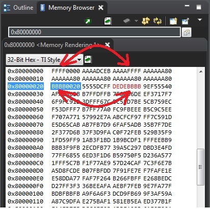
    So far, I have found an interesting thing about the reading/writing to/from the DDR3 memory. After DDR configuration I launch the memory browser with 32-bit hex view and continous refresh. When trying to save something in the respective location, only first half of it is saved in the proper cell - the second half  is saved in the address incremented by 2, as presented below for 0xFFFFFFFF and 0xBBBBBBBB:

     Once again thank you for your answers and I really hope we will figure out how to deal with that problem.

    Best,

    JJ

  • I never said you didn't modify the values. I said the values don't match the spreadsheet. Perhaps you posted an earlier version of your spreadsheet. Please post your gel file and your spreadsheet so I can see that they are consistent.
  • Here is the current GEL file: 

    3480.AM43xx_EMIFconfig_HWlvl.gel

    And here is the current spreadsheet (Biser's settings verified by the DDR manufacturer - I set 11 bits in columns):

    AM43xx_DDR_register_calc_tool TI 400Mhz.xls

    If there is any mismatch between them please instruct us how to correct it.

    Thanks,

    JJ

  • How long are the clock and dqs traces as observed by each of the two DDR3 devices on your board?

  • Hi Brad,

    Do you ask about physical lengths on the board? If yes, they stand as below (CLK_P and CLK_N lines are connected in daisy chain for Memory 1 and Memory2):

    DDR3 Memory 1 DDR_CLK_P 2.565 inch
    DDR3 Memory 1 DDR_CLK_N 2.489 inch

    DDR3 Memory 2 DDR_CLK_P 3.482 inch
    DDR3 Memory 2 DDR_CLK_N 3.448 inch

    DDR3 Memory 1 DDR_DQS0_N 1.458 inch
    DDR3 Memory 1 DDR_DQS0_P 1.457 inch
    DDR3 Memory 1 DDR_DQS1_N 1.247 inch
    DDR3 Memory 1 DDR_DQS1_P 1.247 inch

    DDR3 Memory 2 DDR_DQS3_N 1.454 inch
    DDR3 Memory 2 DDR_DQS3_P 1.454 inch
    DDR3 Memory 2 DDR_DQS3_N 1.448 inch
    DDR3 Memory 2 DDR_DQS3_P 1.448 inch

    Regards,

    JJ

  • - Can you also check from your layout if all the pin connections as shown in the schematic match?

    - It is strange that the errors only occur in the lower bytes and never on the higher bytes. So, looks like we need to focus on the memory part that is connecting to the lower bytes

    - Can you also check if the supply connections and VREF connections are within valid operating ranges? Further, can you probe the signals to see if they look fine?

    Regards, Siva

  • Hi Siva,
    Thanks for your answer.
    We were analyzing the pin connections and traces in the project together with further software trials - accidentally we found out the source(s) of the problem - in the DDR3_ADDRCTRL_IOCTRL_VALUE register only we needed to raise the value of the slopes and the values of the impedance. Does it mean we have some bug in the layout? Does the binary value of 100 really stand for 44Ohms? - so what is the multiplier when setting the impedance in the register?
    Thanks!
    JJ