


Hi team,
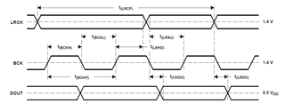
Could you advise a definition of t(LRDO) Delay time, LRCK edge to DOUT valid in Figure 22?
I measured LRCK falling edge to DOUT and the waveform was like the Figure 21 below.
DOUT output at second BCK falling edge, while you can see DOUT is output at 1st BCK falling edge in Figure 22.
Could you advise which is correct?
Figure 21
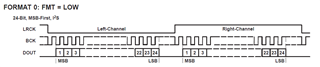
Figure 22
Mode : Slave
I/F : I2S
regards,

