This thread has been locked.

If you have a related question, please click the "Ask a related question" button in the top right corner. The newly created question will be automatically linked to this question.

TAS5756M: Requesting the typical DC Offset Error Threshold and expected tolerance

Part Number: TAS5756M
Other Parts Discussed in Thread: TPA3118D2, TAS5766M

Hello, 

Use Case:
PVDD: 25VDC ± 0.25VDC
Output Configuration: PBTL
Rload: 2.7ohms
Gain/Switching Frequency: 26dBV, 768kHz


We have a several units of TAS5756M devices who are tripping a DC offset error, due to high leakage on the AC coupling capacitors between the DAC output and the IN+ terminal.

We are consistently seeing trip thresholds much lower than 5VDC. Here is a collection of data that we have taken on several units, from several different lots:


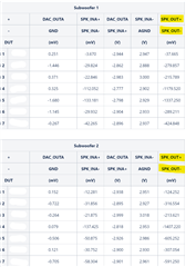
The voltage in the column highlighted was taken on seven different boards and measured differentially from SPK_OUT+ to SPK_OUT- for two TAS5756M ICs on the same board- both of which were configured as per the operating conditions at the top of this post.


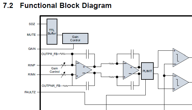
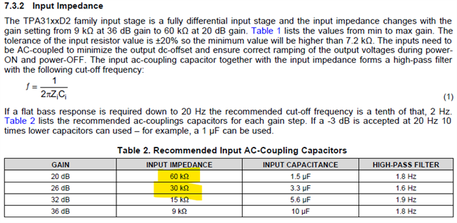
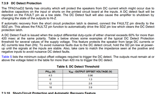
There is no specification for this threshold in the data sheet, and thus we reviewed the TPA3118 data sheet for guidance (since it is very similar to the power stage in the TAS5756M/TAS5766M device). According to the TPA3118D2 data sheet, the value should be over 5VDC, as shown below:

But that is much higher than what we are seeing...

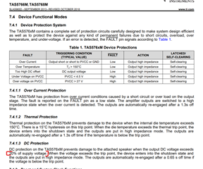
Of course, the TAS5766M device is very similar to the '56M, so we consulted its data sheet as well. It also reports that, since we are using the device at 25VDC on PVDD, we should expect ≈5V of DC offset on the output of the device before tripping a fault:


In further searching we found the popular application note on DC Offset in the TPA31xx family, shown here: https://www.ti.com/lit/an/sloa261/sloa261.pdf

Upon review, this document seems to indicate that the threshold is more like ≈ 2.7VDC 


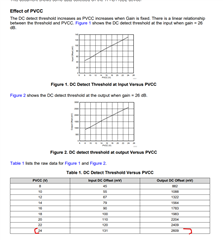
Which is correct, given our operating conditions?

We would also like to know:

  1. What is the nominal trip threshold, given our operating conditions, that we should expect in room temperature?
  2. What is the tolerance for this threshold as measured in the characterization or PTE data (or perhaps the design team can offer some insight)?
  3. Can you please provide min/max data for this parameter from PTE or Char data?

I understand that these values are not published and are not guaranteed, but we are attempting to understand why we are seeing early trip points and need to understand the extent of the issue. It seems that the TPA3118 or the TAS5766 data sheets provide a value which is 1.5x to 2x higher than what we're measuring.

Thanks in advance for your help, and we look forward to hearing from you.

Cody

  • Hello Cody,

    1. What is the nominal trip threshold, given our operating conditions, that we should expect in room temperature? This threshold should be ~2.7V
    2. What is the tolerance for this threshold as measured in the characterization or PTE data (or perhaps the design team can offer some insight)? I would need to speak to the design team
    3. Can you please provide min/max data for this parameter from PTE or Char data? This is not a spec that there is max/min data on

    For the ac coupling caps can you provide the part number you are using? We have encountered in the past significant changes in the past when modifying the AC coupling caps for leakage current improvements.

    best regards,

    Luis

  • Hi Luis! 

    It's great to hear from you. :) 

    Can you help give some context around the 2.7VDC? We are consistently measuring higher than this, and this seems out of aligment with the '66 data sheets' "20% of PVCC" statement. Can you check to see if it changes based upon the switching frequency? I don't think that they characterized that on the TPA31xx app note. 

    For the tolerance, please check with the design team or perhaps the Char/PTE team, since they should have gathered this on one of the predecessor devices. It doesn't have to be exact, but a general sense would be very helpful. 

    It's ok not to specify the min/max- but I think they gather it just for reference. I don't need an official commitment on the min/max, just understanding the risk. 

    For the AC coupling caps, we have addressed the leakage issue caused by the cap, but we have a large number of boards already built, which is the reason I'm trying to understand the min/max/tolerance of the DC detect issue. Thanks for helping track down this issue for us!

  • HI Luis, we are also curious about the differential inputs to to analog back-end of the TAS5756M device. 

    Based on the DC offsets we have observed over temperature, having the following additional information on the TAS5754/6 will be extremely helpful. We suspect that some of this data can be inferred from the TPA3116/TPA3118 and it will be better to know with certainty.

    Verification that the block diagram found in tpa3116 applicable to this series:


    Typical input resistance for 20dB and 26dB modes on the TAS5754, example data from tpa3116:


    For the differential input opamp on the TAS5754, what are the input bias current and input offset current specs? (see below for an example from 33078)

    This following plot will also be helpful too if it is available.


    Thanks in advance for your help!

    Cody

  • Hello Cody, 

    Given the urgency of your request and the need to get additional information from the design team I will follow up this support in an offline email chain rather than e2e.

    best regards,

    Luis

  • Hi Luis, 

    Thank you for your help- that would be much appreciated.

  • Hello Cody,

    No problem and understood, I will continue our communication in the email thread.

    best regards,

    Luis