This thread has been locked.

If you have a related question, please click the "Ask a related question" button in the top right corner. The newly created question will be automatically linked to this question.

TLV320ADC6120: Slave Mode PLL Divider and Selection Registers

Part Number: TLV320ADC6120

To Whom It May Concern,

I would like to program the part to use the PLL configuration show below from the PurePath Console. I didn't see the divider register settings in the data sheet, or in the PurePath Console Register Map. What are the registers, register addresses and register settings to implement the diagram? It looks like these registers would be a PLL input select (MCLK or BCLK), PDIV, J,D, N_DIV, M_DIV, and the 3 input clock MUX select feeding N_DIV. In the system I would be supplying a BCLK at 3.0720MHz and FSYNC at 48KHz.

Thanks,

Shawn

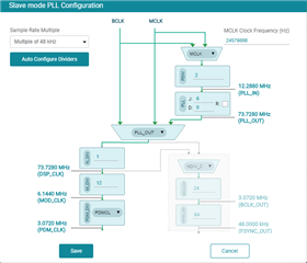
P.S. The register's in the data sheet which appear to be relevant are MST_CFG0, MST_CFG1, CLK_SRC, and PDMCLK_CFG. According to the data sheet descriptions most of the settings are not used in slave mode, auto clock configuration disabled, PLL enabled in Auto Clock Configuration.

  • Hi,

    It seems that the registers that control the PLL factors are not intended to be accessible. The device will either auto configure itself (MST_CFG0) or is supposed to be done through PPC3. If you save the configuration you have, PPC3 should write the proper registers, even if they are technically reserved. 

    Best Regards,

    Jeff

  • Hi Jeff,

     I need to program the part with an FPGA, so using PPC3 is not an option for me. I need to operate the part as a slave and use MCLK as the clock source for the PLL inside the device. My BCLK is noisy since it's sourced from an FPGA. My MCLK is clean since it comes from a crystal oscillator. Is this a viable option with the auto configuration? My interpretation of the register descriptions indicates it is not, but perhaps I am reading it incorrectly.

    Thanks,

    Shawn

  • The PLL auto configuration depends on detecting BCLK and FSYNC ratio. You can read this register  ASI_STS (P0_R21) to see if the device is finding the correct ratio or if the noise is too much of an issue. A workaround may be to use PPC3 and the i2C log to reverse engineer which registers control which values. Even if the registers are not documented, PPC3 has to communicate to the device to change those settings, and those commands should appear in the i2c log. Even without an EVM PPC3 should still attempt to write to the register, and you can work backwards from there.

    Thanks,

    Jeff

  • I would suggest that TI documents manual configuration so the customers do not have to reverse engineer the log file.

    Thanks,

    Shawn

  • The log file doesn't show hidden registers that are programmed.

    .

    config.txt
    typedef unsigned char cfg_u8;
    typedef union {
        struct {
            cfg_u8 offset;
            cfg_u8 value;
        };
        struct {
            cfg_u8 command;
            cfg_u8 param;
        };
    } cfg_reg;
    
    #define CFG_META_SWITCH (255)
    #define CFG_META_DELAY  (254)
    #define CFG_META_BURST  (253)
    
    /* Example C code */
    /*
        // Externally implemented function that can write n-bytes to the device
        // Refer to the device data sheet for more information.
        extern int i2c_write(unsigned char *data, int n);
        // Externally implemented function that delays execution by n milliseconds
        extern int delay(int n);
        // Example implementation.  Call like:
        //     transmit_registers(registers, sizeof(registers)/sizeof(registers[0]));
        void transmit_registers(cfg_reg *r, int n)
        {
            int i = 0;
            while (i < n) {
                switch (r[i].command) {
                case CFG_META_SWITCH:
                    // Used in legacy applications.  Ignored here.
                    break;
                case CFG_META_DELAY:
                    delay(r[i].param);
                    break;
                case CFG_META_BURST:
                    i2c_write((unsigned char *)&r[i+1], r[i].param);
                    i +=  (r[i].param / 2) + 1;
                    break;
                default:
                    i2c_write((unsigned char *)&r[i], 2);
                    break;
                }
                i++;
            }
        }
     */
    
    cfg_reg registers[] = {
    #define CHECKSUM (0)
    // Generated by ADCx120EVM-SW v3.0.5
    // TLV320ADC3120 device configuration
    // -----------------------------------------------------------------------------
    // Reset
    // -----------------------------------------------------------------------------
    // Select Page 0
        { 0x00, 0x00 },
    // Reset Device
        { 0x01, 0x01 },
    // 1mS Delay
    // -----------------------------------------------------------------------------
    // Begin Device Memory
    // -----------------------------------------------------------------------------
    // Page 0 (0x00) Dump
    // Select Page 0
        { 0x00, 0x00 },
    // Wake up and Enable AREG
        { 0x02, 0x81 },
        { 0x05, 0x01 },
    // ASI configuration
        { 0x07, 0x70 },
        { 0x09, 0x20 },
    // ASI Channel configuration
        { 0x0c, 0x20 },
    // ASI master mode
        { 0x13, 0x42 },
    // PDM Configuration
        { 0x1f, 0xb0 },
    // GPIO Configuration
        { 0x21, 0xa0 },
    // DSP Configuration
        { 0x6c, 0x48 },
    // input and output Configuration
        { 0x74, 0xc0 },
    

  • Hi Jeff,

    In the standard mode of operation, it looks like the internal PLL locks to the BCLK signal. Is there phase noise specification on this clock to ensure the ADC's performance is not degraded?

    According to Configuring and Operating TLV320ADCx120 as Audio Bus Controller (sbaa495) I can configure the part to use a crystal oscillator based MCLK which would ensure a low phase noise clock source for the ADC.

    Thanks,

    Shawn

  • Hi Shawn,

    That looks like an i2C dump, which will still only show the intended "unhidden" registers. I was talking about a log that records i2C commands in real time. I agree that it's strange that it isn't documented.

    There isn't a phase noise specification, but you can monitor the ratio on the MST_CFG0 register to tell if it's locking correctly.

    If the crystal oscillator and controller mode is viable for you, I would do that. 

    Thanks,

    Jeff

  • Hi Jeff,

    Thanks! I am going to go with Master Mode and a crystal oscillator. If you find a jitter tolerance or phase noise specification for auto slave mode with the pll enabled please let me know

    Thanks,

    Shawn