This thread has been locked.
If you have a related question, please click the "Ask a related question" button in the top right corner. The newly created question will be automatically linked to this question.
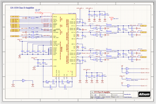
I have a custom PCB with the same schematic of the EVM board.
I'm trying to initialize the chip, I have a workling i2c communication.
But I cannot get any sound from the amplifier.
The i2s signal is generated by the DAC in the PCM9211.
The Main output bus is connected via 33Ohm resisitors to the TAS5731M.
Another DAC (PCM5102a) is connected to another output of the PCM9211 and I have audio.
On a previous thread you sugeste dto get an EVM but it is unobtanium.
I've another product based on the same TAS IC to test out my init init sequence and with that it works.
(See attached init sequence for Logic 2.X below)
I have PVDD set at 12V, AVDD and DVDD are 3.3V.
On bootrap caps I have around 12V. Outputs A,B,C,D are at 6V
ON VREG: 3.1V
On VR_DIG I have: 1.8V
On GVDD_OUT: 7.0V
On SSTIMER: 3.1V
This is the post init register dump of the TAS:
I: Device on address 0x001B I: Device initialized on address 0x001B: 1 V: Going to enable PCM9211 I: Device found on address 0x0040 I: Device initialized on address 0x0040: 1 V: Going to configure PCM9211 I: Main Mux: 2 I: Aux Mux: 2 I: DIT Mux: 4 I: ---TAS5731M------------- I: Reg 0x0000: 0b1101100(0x006C) I: Reg 0x0001: 0b0(0x0000) I: Reg 0x0002: 0b0(0x0000) I: Reg 0x0003: 0b10100000(0x00A0) I: Reg 0x0004: 0b101(0x0005) I: Reg 0x0005: 0b1010(0x000A) I: Reg 0x0006: 0b0(0x0000) I: Reg 0x0007: 0b1001000(0x0048) I: Reg 0x0008: 0b110000(0x0030) I: Reg 0x0009: 0b110000(0x0030) I: Reg 0x000A: 0b110000(0x0030) I: Reg 0x000E: 0b11010001(0x00D1) I: Reg 0x0010: 0b111(0x0007) I: Reg 0x0011: 0b10111000(0x00B8) I: Reg 0x0012: 0b1100000(0x0060) I: Reg 0x0013: 0b10100000(0x00A0) I: Reg 0x0014: 0b1001000(0x0048) I: Reg 0x0019: 0b110000(0x0030) I: Reg 0x001A: 0b1111(0x00F) I: Reg 0x001B: 0b11000000(0x00C0) I: Reg 0x001C: 0b10(0x0002) I: Reg 0x0020: 0b01000100111101111110010(0x0000897772) I: Reg 0x0021: 0b00100000011(0x00000403) I: Reg 0x0025: 0b110100111000101(0x000121345) I: ------------------------
I: ---TAS5731M------------- I: Reg 0x0000: 0b1101100(0x006C) I: Reg 0x0001: 0b0(0x0000) I: Reg 0x0002: 0b0(0x0000) I: Reg 0x0003: 0b10100000(0x00A0) I: Reg 0x0004: 0b101(0x0005) I: Reg 0x0005: 0b1010(0x000A) I: Reg 0x0006: 0b0(0x0000) I: Reg 0x0007: 0b1001000(0x0048) I: Reg 0x0008: 0b110000(0x0030) I: Reg 0x0009: 0b110000(0x0030) I: Reg 0x000A: 0b110000(0x0030) I: Reg 0x000E: 0b11010001(0x00D1) I: Reg 0x0010: 0b111(0x0007) I: Reg 0x0011: 0b10111000(0x00B8) I: Reg 0x0012: 0b1100000(0x0060) I: Reg 0x0013: 0b10100000(0x00A0) I: Reg 0x0014: 0b1001000(0x0048) I: Reg 0x0019: 0b110000(0x0030) I: Reg 0x001A: 0b1111(0x00F) I: Reg 0x001B: 0b11000000(0x00C0) I: Reg 0x001C: 0b10(0x0002) I: Reg 0x0020: 0b01000100111101111110010(0x0000897772) I: Reg 0x0021: 0b00100000011(0x00000403) I: Reg 0x0025: 0b110100111000101(0x000121345) I: ------------------------
Hi
i have some point want to confirm with your problem.
1. no sound been output and no error report be found in0x02.
2. when you change the initial code from another device with same chip, it can output the sound normally? am i understanding right?
3. when you don't have sound, have you confirmed the power supply? input clock signal?
for example: does the MCLK satisfy the timing requirement in the datasheet?
thanks.
Jesse
1) yes, the ABCD OUTPUTs are at 6V (referenced to ground)
2) If I take the same init code and I use it to configure another design based on the same TAS IC I have sound.
3) I've already checked the voltages, and the MCLK is correctly deteced (see register 0x00).
It is coming from a 24.576MHz crystal and divided by two by the PCM9211.
There is some aliasing in the MCLK due to probing wires.
I have a polling loop for register 0x02 that halt the code and show an error via serial.
I also a LED connected to the TAS fault pin, I'm not seeing any error in both cases.
Hi
can you help confirm the signal i marked below.
point1: confirm is there pwm signal, when you playing music, does the duty cycle change or not.
if duty cycle of point1 doesn't change, then confirm point2 is there i2s signal been input to the chip.
2) If I take the same init code and I use it to configure another design based on the same TAS IC I have sound.
here another design using same IC, what about surround circuit of another design? are they the same?
thanks.
Jesse
I'm going to test #1.
About point 2, I've already tested with another I2S source using the PCM9211 to route the I2S bus to the TAS IC.
Also in this case I have no sound.
I'm also going to test if the other I2S source (from the working design) do any effect on this board and I will also try to bypass the PCM9211 IC.
About #1 I have a 50% duty cycle even when sound is playing at around 387kHz. I2S signal is present.
If needed I can provide a capture.
Hi
About #1 I have a 50% duty cycle even when sound is playing at around 387kHz
-> Do you mean when sound is playing, but no sound be heard. ant at this time, the pwm duty cycle is 50%?
Namely, even no sound issue happen, point 1 still have the pwm signal?
it seems like you are using AD mode, can you switch to BD and confirm does it happen or not?
thanks
Jesse
Yes I have no sound, but I2S bus have valid data on it.
PWM is there but is always set at 50% duty cycle.
Company is going to summer vacations, I can see if I can do some last tests tomorrow.
OK, i saw that you said "On bootrap caps I have around 12V" before.
how you measure the voltage, it seems very strange so high bootstrap voltage.
usually it will be 6v~7v.
Hi
Jesse is on business travel for these two days, will reply you as soon as he comes back on Wednesday.
Hi
thank you very much for your confirm.
i checked your original question, you said with other initial sequence, the board worked.
is that possible you initial sequence have any problem?
thanks.
jesse
Hi,
I own a commercial product that is/was (it seems that due to pandemic/chip shortage it has been retired from the shelfs) using 2 TAS ICs in both PBTL and BTL configuration.
I had to find a working design in the market sice I cannot find the EVM board from my available suppliers.
Not the most elegant solution but the only solution we've found.
I've used that product to test out my init sequence (using my MCU and my Init code), and that design works.
I'll have to test if using its I2S source I get any sound on my design. (Ive tested my I2S cource with the commercial product and it works)
My captured init sequence is available in the first post. (you need the logic souite to open it)
In case I can provide some picture.
Hi
i am afraid that i don't have the tool logic souite.
can you share me a screen shot.
thanks.
jesse
Unfortunatly this week i'm out of office, and looks like that the attached dump on first post is incomplete, it only contins the PCM9211 initialization.
Next week I'll provide a screenshot when can I access the right file.
I'm back to office. This is the sequence.
The full init sequence captured by the logic analyzer:
-- OSC TRIM -- write to 0x1B ack data: 0x1B 0x00 -- Soft Mute CH 1/2/4(3) -- write to 0x1B ack data: 0x06 0x07 -- Enable FAULT Pin -- write to 0x1B ack data: 0x05 0x42 -- BD Modulation Configure CH 1/2 -- write to 0x1B ack data: 0x20 0x00 0x89 0x77 0x72 -- BD Modulation Configure CH 4(3) -- write to 0x1B ack data: 0x05 0x4A -- Mode 2.0 -- write to 0x1B ack data: 0x05 0x4A -- Modulation Limit -- write to 0x1B ack data: 0x10 0x07 -- I2S Format 24Bit -- write to 0x1B ack data: 0x04 0x05 -- Channels Delay -- write to 0x1B ack data: 0x11 0xB8 write to 0x1B ack data: 0x12 0x60 write to 0x1B ack data: 0x13 0xA0 write to 0x1B ack data: 0x14 0x48 -- Input MUX Configuration SDIN-L>CH1 SDIN-R>CH2-- write to 0x1B ack data: 0x20 0x00 0x89 0x77 0x72 -- Input MUX Configuration CH4(3)>L+R/2 -- write to 0x1B ack data: 0x21 0x00 0x00 0x40 0x03 -- DAP CH4(3) to 3rd volume control -- write to 0x1B ack data: 0x0E 0xD1 -- Channel volumes to 0dB -- write to 0x1B ack data: 0x08 0x30 write to 0x1B ack data: 0x09 0x30 write to 0x1B ack data: 0x0A 0x30 -- Exit Hard Mute -- write to 0x1B ack data: 0x05 0x0A -- SoftMute Master Volume -- write to 0x1B ack data: 0x07 0xFF -- Soft UnMute CH 1/2/4(3) -- write to 0x1B ack data: 0x06 0x00 -- PCM9211 INIT -- -- END OF PCM9211 INIT -- -- Set Master Volume (-12dBm) -- write to 0x1B ack data: 0x07 0x48
Hi
i noticed that you set your master volume -12dB, is that possible the Gain is too small so that sound cannot be heard?
how about adjust it a little larger?
another problem is :
-- Soft UnMute CH 1/2/4(3) --
write to 0x1B ack data: 0x06 0x00
I checked register 0x06, if unmute ch 1,2,3, it should be 00000111, so namely 0F.
can you help confirm whether this is a problem?
thanks
jesse
I'm going to try to increase the master gain.
About the channel mute register.
I initially mute them by writing 0x7 (in the beginning after OSC TRIM),
but after to unmute them I need to write 0x00 according to the table you provided.
Have I misinterpreted that table?
Oh, sorry for i misunderstanding your code.
your understanding is right. then the initial code seems no problem.
Ok, so to remuse:
Code seems to be ok and my startup sequence seems fine.
The schematic seems correct, how about the PCB layout?
We have designed a simpler board just to evaluate the TAS chip
without the PCM9211.
But we are also considering to completly scrap the design based on this chip.
Hi
i confirmed that your inductance for LC filter current saturation and current rating is 3A and 2.5A.
your pvdd is 12v, can you inform me the resistance of your load?
BTW, can you measure the current go through the inductance when you startup your device?
you can using wire connecting the inductor, can clip the current sense around the wire to measure the current.
i am afraid that the current saturation is not enough so that no sound happen.
thanks.
Jesse
My load is a 6 Ohm driver, I've also tried with a 8 Ohm one.
I've tried to increase the supply voltage (PVDD) to 24VDC.
Now I can barely hear some voices coming from the driver but nothing more.
I can confirm that I have modulation and I can see the signal/duty cycle changing when sound is present in the bus
(see attached video).
Probe is x10, 0.5V/DIV, 2us/DIV.
Ground lead was long so not the better signal integrity.
I've also tried to tweak the board to remove the Cbtl to have a proper filter for the BD modulation as you suggested. (filter was designed for AD modulation with hybrid design)
I've used the excel file to calculate a new filter, I settled for a Cg with a value of 0.68uF while keeping the 22uH inductor.
During this test I was using a 8Ohm driver.
With this new filter I was getting an even lower volume.
I'm going to test the inductor current tomorrow. Isn't the current stay below saturation threshold?
Otherwise the impetence of the inductor would collapse?
Hi
it seems like your problem now become volume too small. not no sound, am i understanding right?
according to your waveform, it seems like no problem with your output.
i noticed the code you give me last time.
-- Set Master Volume (-12dBm) --
write to 0x1B ack data: 0x07 0x48
it seems like you set the master volume -12dB, am i understanding right?
is that possible your volume setting in your software is too small to hear the sound?
when you run the device, does the inductor become very hot or not?
if it is very hot, i am afraid that maybe the current go through inductor is too large so that the effective inductance value become small.
thanks.
Jesse
The master volume has been set at 0dB to be able to hear anything.
After 5 Minutes the inductors are cold to touch. The IC is sightly warm.
With "barely hearing" the sound I mean that I have to put a 5 inch driver near my ear in a perfect silent enviroment and then I can pickup some words. An ear phone in a noisy bus make more sound that this.
thank you very much for your confirm.
it is not very hot, then the current should be not very large.
it seems like you have the output to the speaker. Have you confirmed the signal at both side of speaker? how much voltage been outputted now?
for this chip is too old, i am trying to get an EVM board, after i got one, i will use your initial code to confirm this issue.
thanks.
Jesse
Test coditions:
- PVDD=24V
- Load 8Ohm (Driver model: DS90-8)
- LC filter: common mode, 22uH, 0.68uF
- BD modulation
I reduced all the init code to:
- OSC trim
- delay
- set BD modulation
- set delays
- exit hard mode
- set master gain to 0.
The result is as before.
Measurements:
- 11.25V on OUT(ABCD),
- PWM signal is modulated on OUT(ABCD). Singlal is as shown above.
- Post LC filter I have an analog singnal (see picture). The signal is 11Vpp referenced to GND (5V/DIV)
- All the outputs have a similar signal amplitude.
- PVDD is stable, some HF noise is present due to the SMPS converter.
- I basically don't have any voltage across the driver. (cannot measure anything, this made me check the phase of the outputs)
OUT-A (post LC filter, referenced to GND)
OUT-A and OUT-B (before LC filter, referenced to GND)
Sorry for the picture with wrong angle,
but for some odd reason they are right on my machine,
once uploaded they are 90 degree off.
Is that PWM singnal correct?
By reading SLAA701A I was expecting a different waveform.
If I use diff/sum mode of the oscilloscope on OUT A and C I get the following waveform, but OUT A is driven by channel-L and OUT-C is driven by channel-R:
This is something more similar to the modulation showed in the SLAA701A.
How can this be possible?
The dump of Register 0x25 is:
I: Reg 0x0025: 0x0001021345
I never set that register, and it is at its default.
My init code is:
// CHIP reset gpioWrite(_rstPin, 0); // Await 15 ms before exit reset delay(15); gpioWrite(_rstPin, 1); // Await 15 ms before trim delay(15); // Run a factory OSC TRIM as stated in datasheet ret = write8(TAS571X_OSC_TRIM_REG, 0); if (ret) { Log.error(F("Could not set OSC_TRIM: %d\n"), ret); return ret; } // Lets wait 50ms delay(50); // Set chan 1, 2, 3 (4) delays to default values res |= write8(TAS571X_IC_DELAY_PWM_A_REG, 0xB8); res |= write8(TAS571X_IC_DELAY_PWM_B_REG, 0x60); res |= write8(TAS571X_IC_DELAY_PWM_C_REG, 0xA0); res |= write8(TAS571X_IC_DELAY_PWM_D_REG, 0x48); if (ret) { Log.error(F("Could not set DELAY_PWM: %d\n"), ret); return ret; } // Exit Hard Mute (shutdown) ret = updateRegister8(TAS571X_SYS_CTRL_2_REG, TAS571X_SYS_CTRL_2_SDN_MASK, 0x00); if (ret) { Log.error(F("Could not set VOL_CFG: %d\n"), ret); return ret; } // Lets wait 50ms delay(50); // Set Master Volume ret = write8(TAS571X_MVOL_REG, 0x30); if (ret) { Log.error(F("Could not set master volume: %d\n"), ret); return ret; } return ret; }
Just to confirm I've done a similar scope probe to the working commercial product (this time I was using its MCU to perform the initialization. it uses BD mode. I have captured their init sequence and it is almost identical except for modulation limit and they also set BEQs and DRCs).
The two OUTA and OUTB are out of phase (first picture), meanwhile our design the two outputs are almost in phase (second picture):
Hi
The waveform shows our device works in idle state, and seems your register setting shows the device shouldn't in Mute state. Can we capture the waveform of SDIN, together with LRCLK and SCLK when Playing the audio. Hope we may find something strange.
The capture of the post above was done in both cases with a paused/muted source as ingress.
This is the logic capture of the I2S bus. The MCLK is out of the range of my logic analyzer.
The BCLK has an some sort of periodic artifact, but I cannot see it in the scope. I think that the issue is with my capture device (long probing cables and bad ground.
BCLK, MCLK (is quite near my SCOPE limit), WS, SDIO:
All the signals are around 3Vpp (1V/DIV). MCLK and BCLK had a .4us/DIV, while the WS was at 20us/DIV.
BCLK VS WS (1V/DIV 2us/DIV):
Hi
I tried your code, it doesn't work on our EVM board, i am not very sure it is format issue or the code issue.
But I used our EVM board and configured a default setting.
it worked and initial file was dumped.
can you transform the cfg file attached to your format and take a try whether it work or not?
/cfs-file/__key/communityserver-discussions-components-files/6/i2c-initial-file_5F00_nomute.cfg
if you have our EVM baord, you can also use below link setting file to confirm the setting.
/cfs-file/__key/communityserver-discussions-components-files/6/GDE_5F00_file.zip
thanks.
Jesse
We dont have the EVM.
I have updated my code to output the sequence you provided:
void tas_init() { gpioOutput(TAS_PDN_PIN); gpioOutput(TAS_RST_PIN); gpioWrite(TAS_PDN_PIN, LOW); gpioWrite(TAS_RST_PIN, LOW); // Await 15 ms before exit reset delay(15); Log.info(F("Power Sequence\n")); gpioWrite(TAS_PDN_PIN, HIGH); gpioWrite(TAS_RST_PIN, HIGH); delay(15); Log.info(F("Trim\n")); write8(TAS571X_OSC_TRIM_REG, 0x00); delay(50); Log.info(F("Inits Core\n")); // soft unmute write8(TAS571X_SOFT_MUTE_REG, 0x00); Log.info(F("Inits Volumes\n")); write8(TAS571X_CH3_VOL_REG, 0x30); write8(TAS571X_CH2_VOL_REG, 0x30); write8(TAS571X_CH1_VOL_REG, 0x30); Log.info(F("Inits Delays\n")); // AD Modulation here write8(TAS571X_IC_DELAY_PWM_D_REG, 0x54); write8(TAS571X_IC_DELAY_PWM_C_REG, 0xAC); write8(TAS571X_IC_DELAY_PWM_B_REG, 0x54); write8(TAS571X_IC_DELAY_PWM_A_REG, 0xAC); Log.info(F("Inits Volumes\n")); write8(TAS571X_VOL_CFG_REG, 0x91); Log.info(F("Input Mux\n")); // AD Modulation write32(TAS571X_INPUT_MUX_REG, 0x00017772); write8(TAS571X_MODULATION_LIMIT_REG, 0x02); //IDK - reserved register? write8(0x0B, 0x00); write8(TAS571X_MODULATION_LIMIT_REG, 0x02); write8(TAS571X_BKND_ERR_REG, 0x02); write8(TAS571X_PWM_CH_SDN_GROUP_REG, 0x30); write32(TAS571X_PWM_MUX_REG, 0x01021345); // Bypass EQ write32(0x50, 0x80); write8(TAS571X_SYS_CTRL_2_REG, 0x00); // Uncomment to hear something // write8(TAS571X_MVOL_REG, 0x30); }
This is the capture of the I2C bus:
write to 0x1B ack data: 0x1B 0x00 write to 0x1B ack data: 0x06 0x00 write to 0x1B ack data: 0x0A 0x30 write to 0x1B ack data: 0x09 0x30 write to 0x1B ack data: 0x08 0x30 write to 0x1B ack data: 0x14 0x54 write to 0x1B ack data: 0x13 0xAC write to 0x1B ack data: 0x12 0x54 write to 0x1B ack data: 0x11 0xAC write to 0x1B ack data: 0x0E 0x91 write to 0x1B ack data: 0x20 0x00 0x01 0x77 0x72 write to 0x1B ack data: 0x10 0x02 write to 0x1B ack data: 0x0B 0x00 write to 0x1B ack data: 0x10 0x02 write to 0x1B ack data: 0x1C 0x02 write to 0x1B ack data: 0x19 0x30 write to 0x1B ack data: 0x25 0x01 0x02 0x13 0x45 write to 0x1B ack data: 0x50 0x00 0x00 0x00 0x80 write to 0x1B ack data: 0x05 0x00
I had to set the master volume to 0dBm as the init sequence you provided was not setting that. (without that i cant hear anything)
I've tried with both AD and BD modulation, the result is the same.
Hi
that is so strange.
is that possible your input is too small?
i checked your i2s signal, what kind of signal you used, it seems like it's not sine wave.
BTW, below link is our EVM board related circuit and information.
maybe it can be you reference.
thanks.
jesse
Hi,
I know that is is really strange.
About the input beeing too small one of my alternative sources is a PCM2706 is is directly connected to the I2S bus of the TAS. I bypassed the PCM9211.
The USB chip is connected to a windows machine, volume is set at 100% format is 16bit 44Khz. I've recofigured the TAS to work with 16bit words and the result is as above a really tiny sound.
Other than that during the previous tests I used the PCM9211 internal ADC. (if needed I can share the init sequence of that IC too)
But basically I configured its ADC it in standalone mode, 44kHz with a gain of +12dBm. The PCM9211 is outputting to both its main bus and the "ausiliary" one (MPIOB if I remember correcly). The MPIOB is connected to a PCM5102A for development purposes and that DAC is correctly able to output a strong analog signal.
Yes that screen capture was showing a song playing, not a sinewave. I've tested also with a signal generator but the result is as always a very low volume. If necessary I can provide a capture of a sinewave at 1kHz.
Tomorrow we are going to exclude the possibility that the issue is due to the 22uH inductance by switching it to a 15uH one.
I'm starting to wonder if the CHIPs we got are defective in some way. The desing is based on the EVM file you provided with the exception of the LC filter that has been calculated using the excel file from your documentation.
The PCB layout can be seen in the first post, the LC filter stage design/layout is identical to the redesign we shared some post ago.
I mesured again across the speaker via a TRUE RMS voltmeter and I get around 80-100mV. (it varies based on the sound of the I2S bus. 100mV is with a 1kHz squarewave, any other signal is lower)
We also noted that the capacitors of the LC filter using a squarewave (ceramic through hole) vibrates due to the piezoelectic effect and they output more "sound" than the driver itself.
We started to do our test during after hours to have more silence, the day room noise foor make impossible to hear anything.