This thread has been locked.

If you have a related question, please click the "Ask a related question" button in the top right corner. The newly created question will be automatically linked to this question.

TLV320ADC6120: SINGLE ENDED CONFIGURATION PROBLEM

Part Number: TLV320ADC6120

Hello, I'm developing an acquistion board using the TLV320ADC6120

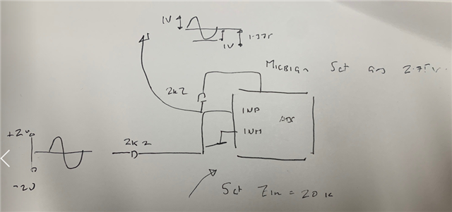
I have an input  signal with amplitude +/- 2Vpp cetered at 0V.

I used MICBIAS/2  output to shift the signal to the range 0-2.75V, is it correct to use this output to create the Common mode voltage?

I need to have a DC coupled signal.

I configured the ADC in sigle ended input  mode DC coupled. (IN1P, IN1M=GND), is it correct?

The digital signal I acquire seem to be saturated in the upper side, if I configure the channel as DIFFERENTIAL mode I see the aspected output.

I'm also in trouble with  configuration register BIAS_CFG Register (Address = 0x3B) what is the meaning of VCM cited in the table 8-84? Can I use MICBIAS with VCM level to  shift my signal?


  • What is the DC Couipled circuit you are using?

    Perhaps you could try the below arranmgement and see if it works

  • it is a really interesting solution, I used classic opamp summing config to shift the signal.

    If I configure the ADC channl as DC coupled SINGLE ENDED, from the digital point of view it seem to have the signal translated of about 2 Vocm.

    IF I configure the ADC in differential mode I see the output signal as expected.

    Second question: In order to use the internal PGA I need to enter in diiferential mode, is it correct?

  • Shall reply in a short time

  • For DC Coupled operation i would suggest to set Vref to 2.75v with Page 0 R59. Then with you OP Amp level level shift, set the no signal Voltage at ADC INP+ Pin to Vref/2(1.375).

    If you now give a 1VrmS around this 1.375v bias signal signal with Channel Gain of 0db you should see a proper output . 

    The Internal PGA should be available for single ended input also

  • When I set a gain to the PGA, all the input signal are amplified (DCBIAS+AC componnet). 
    I confirm you that R59 is configured to obtain 2.75V.
    I double check for the configuration I made but it seem to don't works with SINGLE ENDED channel configuration.

    here below the configuration I'm using 

    AdcCfgReg_t ADregistersInit[] = {
    // Generated by ADCx120EVM-SW v3.0.5
    // TLV320ADC6120 device configuration
    // -----------------------------------------------------------------------------
    // Reset
    // -----------------------------------------------------------------------------
    // Select Page 0
    { 0x00, 0x00 },
    // Reset Device
    { 0x01, 0x01 },
    // 10mS Delay
    { CFG_META_DELAY, 10 },
    // -----------------------------------------------------------------------------
    // Begin Device Memory
    // -----------------------------------------------------------------------------
    // Page 0 (0x00) Dump
    // Select Page 0
    { 0x00, 0x00 },
    // Wake up and Enable AREG QCHAGRE 100ms
    { 0x02, 0x99 },
    { CFG_META_DELAY, 10 },
    { 0x05, 0x01 },
    // ASI configuration
    { 0x07, 0x70 },
    { 0x09, 0x00 },
    // ASI in SLAVE mode
    { 0x13, 0x02 },
    { 0x14, 0x44 },
    { 0x16, 0x00 },
    // ASI Channel configuration
    { 0x0B, 0x00 },
    { 0x0c, 0x20 },
    { 0x0d, 0x00 },
    { 0x0e, 0x00 },
    // PDM configuration
    { 0x1F, 0x40 },
    // GPIO Configuration
    { 0x21, 0x00 },
    // BIAS CONFIG AND ADC FULL SCALE
    { 0x3B, 0x00 }, // 0x50 -> ADC(0:1) full scale 0 -> 2.75V 1 -> 2.5V 2 -> 1.375V, MICBIAS set to VCM //0x00 MICBIAS set to VREF
    // Channel 1 configuration
    { 0x3c, 0x98 }, //0x98 = differential input, impedance 20kOhm //0xb8 = single ended
    // Channel 2 configuration
    { 0x41, 0x98 }, //differential input, impedance 20kOhm
    // GAIN Config
    { 0x71, 0x00 },

    // DSP Configuration
    { 0x6b, 0x00 }, // 0x01 HPF INPUT FILTER ENABLE AT 12Hz
    { 0x6c, 0x00 },
    // input and output Configuration
    { 0x74, 0xc0 },
    // Select PAGE1
    { 0x00, 0x01 },
    //VAD Config
    { 0x1E, 0x00 },
    { 0x1F, 0x00 },
    //Select page 0
    { 0x00, 0x00 },
    //POWERUP CONFIG
    { 0x75, 0xf0 },
    // END TABLE
    { CFG_META_END, 0xFF },
    };

  • 6120_0DB.cfg6120_10DB.cfg

    I MADE 2 FILES FROM OUR PURE PATH 3 TOOL . ONE FILE SETS A GAIN OF 0DB, THE SECOND A GAIN OF 10DB.

    You can give LRCLK of 48k and BCLK of 3.072 Mhz to the Device.

    Let me know if this helps. Alo please send me the schematic