This thread has been locked.

If you have a related question, please click the "Ask a related question" button in the top right corner. The newly created question will be automatically linked to this question.

TLV320ADC6120: SINGLE ENDED CONFIGURATION

Part Number: TLV320ADC6120
Other Parts Discussed in Thread: ADC6120EVM-PDK

Hi all,

I am following up the related question (sorry for the late feedback).
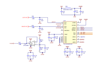
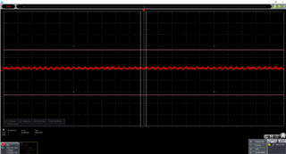
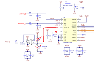
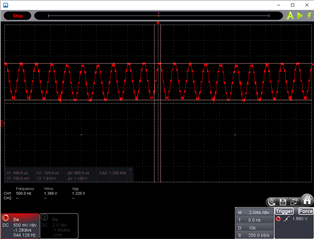
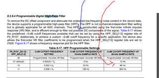
I tried the configuration provided by , and the signal seems to be centered at 0 and not clipped, but looking for the differences with our configuration we find out that there is the high pass filter at 12 Hz enabled, that is not suitable for our application.

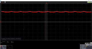
Thanks to this test we realized that the ADC is clipping the signal after the filter, is that correct?

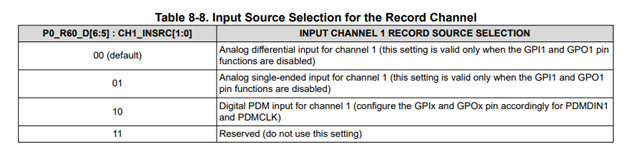
I have another question about the MICBIAS configuration: the configuration MBIAS_VAL = 2 to 4 are descripted in the R59 description but are given as "Reserved (do not use these settings)" in the Programmable Microphone Bias paragraph. Can the configuration "4d = Microphone bias is set to VCM = average of IN1M and IN2M, for ADC single-ended configuration" be a solution for our set-up?

Thanks,

regards

Arianna

  • Would you please send me your input circuit?

  • Hi Sanjay,

    here it is our input circuit:

    LEFT-CH and RIGHT-CH are our input signals (+/- 2Vpp).
    VOCM is fed back to the left channel and right channel amplifier.
    Our VREF is not given by the VREF pin as in the image but from the MICBIAS pin.

    Let me know if you need more info.

    Thank you,

    regards

    Arianna

  • Are LEFT-CH and RIGHT-CH riding on a DC Bias. can you please send me a snapshot of the waveform on pin 1 and pin 3. Please put oscilloscope on DC Coupling for the measurement.

    Also I did not understand the below statement.. 'Our VREF is not given by the VREF pin as in the image but from the MICBIAS pin'. Can you please explain?.

  • Hi Sanjay,

    I took the snapshots on pin 1 (it is the same on pin 3).

    If I set MICBIAS = VREF (reg 0x3b = 0x00), I see this:

    so the signal is, as expected, riding on a VREF/2 bias, but the ADC is not reading something near 0, but something near 2^31.

    If I set MICBIAS = IN1M (reg 0x3b = 0x20), I see this:

    so the signal is centered at 0, that is the same value that I read from the ADC.

    If I apply a typical signal in this configuration:

    I see in the digital converted data also the negative part, so it seems that the ADC is expecting also a negative signal!

    Regarding the MICBIAS sentence, we actually modified the input circuit like this:


    Thank you for your help,

    regards,

    Arianna

  • 1.Are you writing on register 0x3C the value 0x30?

    This should set up the Analog single ended input with DC Coupling.

     2. Set MICBIAS = VREF (reg 0x3b = 0x00)- As you have already done  

          This will set MICBIAS at 2.75v 

            Vref at 2.75v

           As I see in your schematic the output of the Buffer op amp is Vref. Do you divide it by 2 in your circuit to get Vref/2 on input pin?

    After writing settings in 1 and 2, please apply a 1Vrms signal at 1khz . Would it be possible to sent a Plot of the digital Data?

  • Hi Sanjay,
    I was setting 0x3c = 0xb8 (line input, 20 kOhm of impedance). Now I set it to 0x30 as you suggested.

    The signal we need to record cannot reach the parameters you suggest, so I did the acquisition with a signal at 500 Hz and 1.3Vpp:
    This is pin 1 snapshot:


    and this is the digital recording:

    As you can see, the upper part seems to be digitally clipped.

    Regarding your question, yes, the Vref voltage is divided by two in order to have Vref/2 as common mode voltage of the signals.

    Thank you,

    regards

    Arianna

  • shall reply on monday.

  • 1.Would you please try the High CMRR Mode in the above register?

    2.Also, what is the Voltage of th Highest point on the sine wave on the input pin is your sope shot? I cant make out for sure?

    3.You can also do an experiment by removing the input of the op-amp from the MicBias point. Connect it to a DC Voltage and vary this voltage to a value inder

    4.Vref. Then see if there is a point where the clipping goes away. This might help us to get to the issue you face

  • Also, the below was something you mentioned below.  Do you mean that my initial configuration was giving a non clipped output?Can you please elaborate?

    I tried the configuration provided by , and the signal seems to be centered at 0 and not clipped, but looking for the differences with our configuration we find out that there is the high pass filter at 12 Hz enabled, that is not suitable for our application.

  • Hi Sanjay,

    1. Do you mean R58? Which value of impedance do you suggest to use?

    2. The highest value is 1.91 V and the lowest 750 mV

    3. I will check with the hardware department if they can help me for this test, but it will take some time.

  • Yes, if I keep the high pass filter enabled (R107 = 1) the signal is centered at 0 and not clipped.

    regards

  • Hi Sanjay,

    to bypass our hardware limitations, we arranged a new setup, using a ADC6120EVM-PDK and a function generator connected to IN1 connector.

    We started from the preset 'Single-Ended Line Input', with the following jumper configuration:

    - open: J12, J15, J19, J17, J16, J13
    -shorted: J7, J6, J5,J4


    Setting the high-pass filter to a 'all-pass' filter, we see the same issue:
    - Scope snapshot (1Vrms with a DC offset of 1.375V, 1kHz):

    - Digital representation snapshot (0 is where there is the black arrow on the right):


    To perform the experiment you asked, we reduced the DC offset, but, keeping the 1Vrms amplitude, we see clipping until the DC offset is 0 V.

    Using this setup, we noticed that both IN1M and IN1P kept floating have a voltage = VREF/2, and if we don't short the IN1M with the GND pin, we see a digital 0 output. When we short IN1M and GND pin (with IN1P still floating), we see a continuous digital signal near the digital maximum.

    So it seems that also in single-ended the ADC is working as differential, only with a different amplification! Is it a wrong interpretation?

    Thank you,

    regards

    Arianna

  • 1. Is the selection  single ended DC Coupled Mode. 

    2.What exactly do you mean when you say DC offset of 0v. Do you mean we have a signal with a positive peak of 1.4v and a Negative Peak of -1.4v?

    -------------

    I am thinking that In Single ended Mode the DC voltage of Vref/2  is treated as a signal. Passing it through a High pass filter removes this DC component.

    Does a 1Vrms centred on Vref/2(1.375v) with High Pass filter enabled give Proper output ?

    .

    if you like to use the All pass filter switched  with your circuit perhaps you can try Putting Vref/2 on INM pin and feed the  1V rms signal to INP pin with the offset of 1.375v. Put input in differential mode

  • 1. Is the selection  single ended DC Coupled Mode.

    Yes.

    Do you mean we have a signal with a positive peak of 1.4v and a Negative Peak of -1.4v?

    Yes, obviously the signal appears distorted, but Vref/2 seems to be the max allowed voltage.

    Does a 1Vrms centred on Vref/2(1.375v) with High Pass filter enabled give Proper output ?

    Yes.

    if you like to use the All pass filter switched  with your circuit perhaps you can try Putting Vref/2 on INM pin and feed the  1V rms signal to INP pin with the offset of 1.375v. Put input in differential mode

    I agree that it is the way, I report the results of our tests, hoping that they can be useful for someone else..

    Test 1:

    • IN1M floating (= 1.375V)
    • IN1P = sine @1kHz, 1 Vrms centered at 1.375V
    • Single ended -> digital signal goes from -100% full scale to 100% full scale
    • Differential -> digital signal goes from -50% full scale to 50% full scale

    Test 2:

    • IN1M shorted to GND
    • IN1P = sine 1kHz, 1 Vrms centered at 1.375V
    • Single ended -> digital signal goes from 0% to 100% full scale but the higher part is clipped (only half of the signal is shown)
    • Differential -> digital signal goes from 0% to 100% full scale

    Test 3:

    • IN1M shorted to GND
    • IN1P = sine 1kHz, 0.5 Vrms centered at 0.687V
    • Single ended -> digital signal goes from 0% to 100% full scale, not clipped

    So, for our application we have 3 choices:

    • patching our hardware to keep the INM pins floating
    • use MICBIAS/4 as Vocm and manage only 500 mVrms
    • set the ADC as differential and still manage 1 Vrms (we will go probably with this one)

    then we will change our input circuit for the next hardware release.

    Thank you for your help,

    kind regards,

    Arianna