This thread has been locked.

If you have a related question, please click the "Ask a related question" button in the top right corner. The newly created question will be automatically linked to this question.

PCM1863: Timing Requirements

Part Number: PCM1863

Hello,

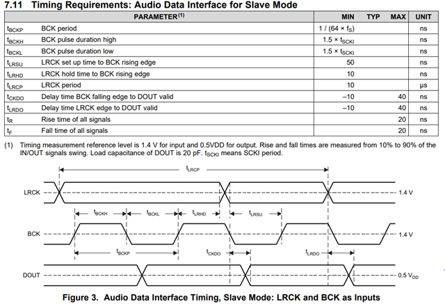
On the datasheet, Section 7.11 Timing Requirements.

(1) tBCKL min is 1.5x tSCKI.

In our customer's usage is I2S slave mode with PLL BCK input.

At this case, SCKI is not used but internal PLL generate SCK.

Should we convert your requirement to 1.5x tSCK?

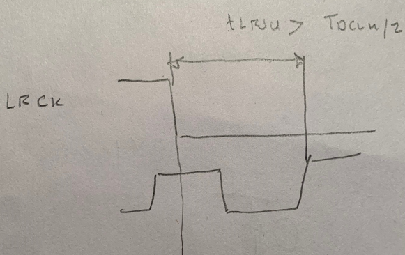
(2) tLRSU min is 50ns.

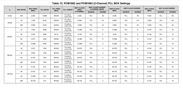
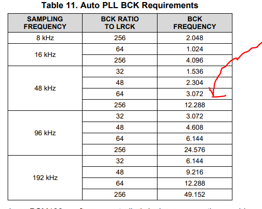
At 192KHz sampling data, LRCK cycle is 81.4ns and setup time become 40.7ns.

We cannot meet tLRSU requirements, what is reason of this discrepancy.

(3) tLRDO = -10 ~ 40ns

At Fs48KHz 64BCK condition, actual capture of the device output tLRDO is 320ns.

What is reason of this difference?

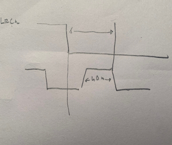
(4) tLRHD threshold LRCK is 1.4V and BCK is 1.4V

But the drawing of LRCK threshold looks 90% point, which is correct?


Regards,

Mochizuki

  • Can you please send me the specific BCK and LRCK Timings you like to support ?

  • (1) If customer is using PLL BCK Input then they have to just apply BCK and Fs as indicated by Table below. The Chip shall

    automatically generate the Internal Clocks. PLL is always turned on as can be seen by the timings below.

    2. From what i see you use a sampling RateFs=192 Khz and a BCK of 12.288Mhz to get a ratio of BCK/FSYNC of 64.

    This gives Tbclk=81.3ns. Tblk/2=40.6ns

    To my mind in Slave Mode  the the Incoming timings are always such that the LRCK is counted down from the BCK.

    If the BCK Rising edge is a trigger to make  the LRCK then the 

    LRCK Transition comes after BCLK rising edge. The next Rising edge comes almost Tblk Time later.

    Thus the TLRSU can be greater then 50ns.

    3. At Fs48KHz 64BCK condition, actual capture of the device output tLRDO is 320ns.

    Is the 320ns a measurement? Can you describe the test in that case? I ask because its always possible that the First bit is a Zero. At 48K/64BCK ,BCK=3.072Mhz .Each bit time IS 320 ns.

    Therefore its possible that there is no data on the first bit.

    Please check Rx_TDM_OFFSET

    4.

    tLRHD threshold LRCK is 90% and BCK is 1.4V. This is the timing as defined in the image

  • Hi Sanjay,

    Thank you for your support.

    (1) Our customer’s configuration is fs=48KHz 64BCK mode in table12. Our concern is that in the case of PLL mode, SCKI input clock is not needed. Then BCK timing “tBCKL min is 1.5x tSCKI” requirement is not satisfied. Can we expect there is no requirement of BCKL min timing during PLL mode?  

    (2) Depend on I2S master processor, some case BCK falling edge is trigger to LRCK edge. Like below timing chart which is on the datasheet. In this case “tLRSU min is 50ns” can be relaxed to accept 40.7ns at fs-192KHz?


    (3) You are correct, we use I2S mode which has 1BCK delay.

    (4) Foot note said “(1) Timing measurement reference level is 1.4 V for input and 0.5VDD for output. Rise and fall times are measured from 10% to 90% of the IN/OUT signals swing.”  From this statement we think BCK and LRCK timing should be 1.4V point and the drawing is something shifted.

    Regards,

    Mochizuki

  • I shall respond tomorrow(03/23)

  • With 48kHZ/64BCK mode a BCK Frequency of 3.072Mhz is needed. Thats all we need.

    If the LRCK is triggered from the Falling edge the same should apply.

    Lets say the falling edge of BCK is sampling edge

    the Time is measured from the falling edge of LRCK to the falling edge of BCK. 

    the falling edge of LRCK would have come some time after the last falling edge of BCK. We thus get more then 40ns.

    ---------------

    You can use TLRHD as a minimum value.