This thread has been locked.

If you have a related question, please click the "Ask a related question" button in the top right corner. The newly created question will be automatically linked to this question.

OPA1622: Weird Line Driver

Part Number: OPA1622
Other Parts Discussed in Thread: LM4562, OPA211, OPA210, THS4031, OPA1612, , OPA828, OPA2210, OPA1637, LME49860, THP210, TINA-TI, OPA1602

Would this work IRL? Anything to look out for? Suggestions for improvement?

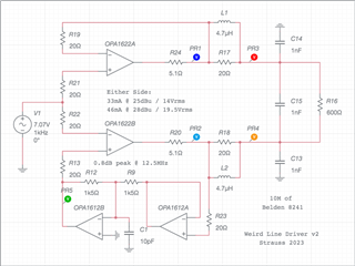
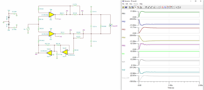
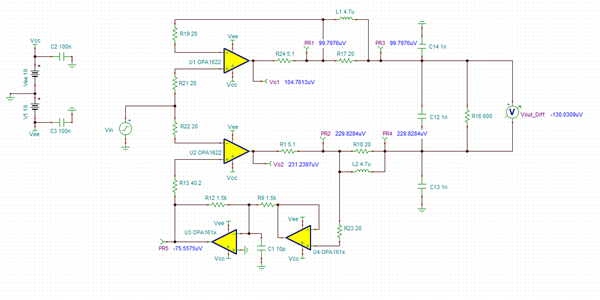
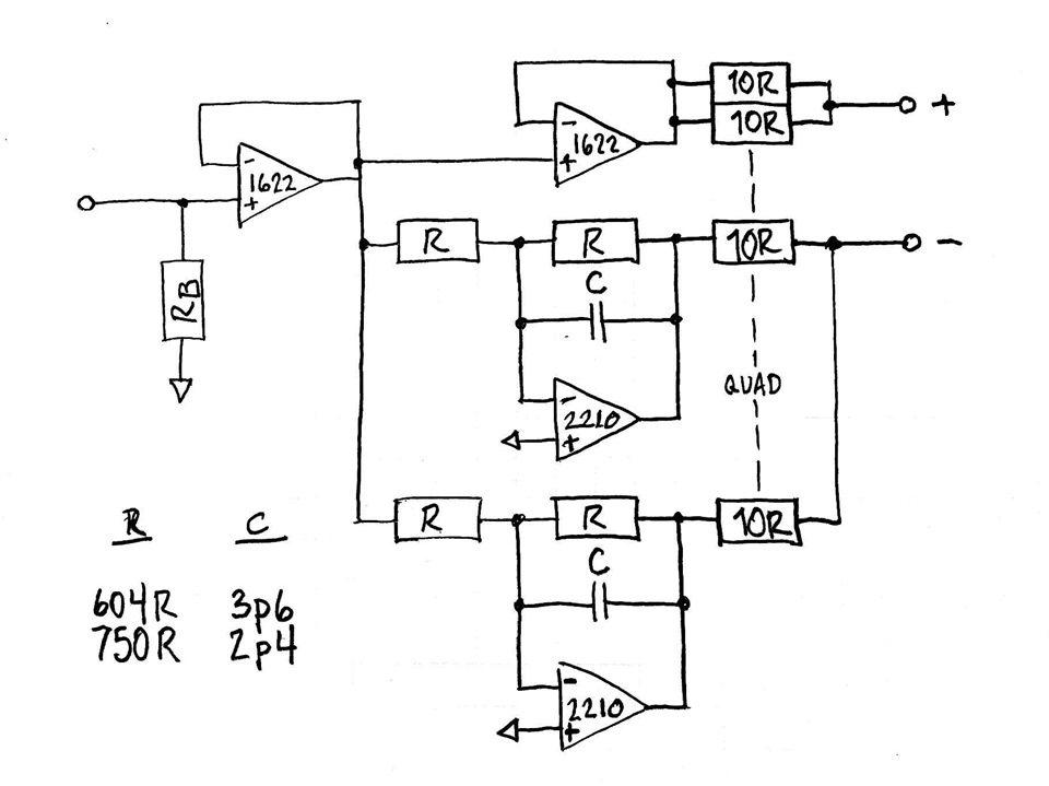
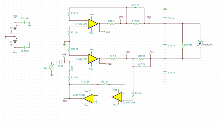
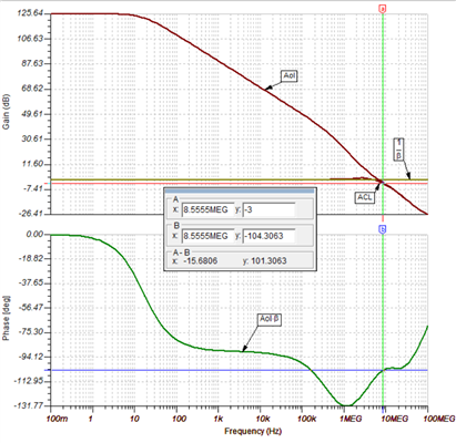
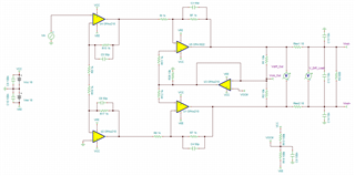
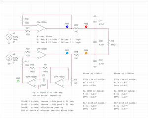
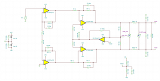
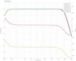
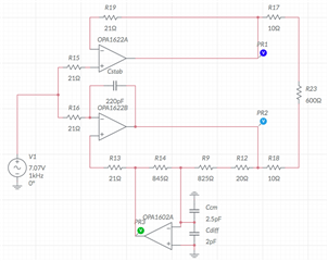
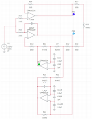
• The ideal amp for the duty the OPA2211 is performing here would run at a minimum of 40MHz, or ≥20MHz at Av=-1. Elimination of inverting 1622 peaking around 8MHz involves running the 2211 without any Cf -- even at Rf=604R and Cf=5p6 there's a 1.7dB peak. Normally the Cf omission would be verboten, but I suspect resultant peaking at the 2211 output might actually be an advantage in this scenario, as it would turn any 1622 peaking down if the peaks were in the same neighborhood. The LM4562 is a little faster and is thus more effective at eliminating 1622 peaking (about 0.8dB vs the 1.7dB I mentioned), but it would limit output capability on ±15V supplies, which this is designed for.

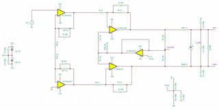
• An alternate method of achieving inverting 1622 flatness involves a composite amp with a single unity inverting OPA211 (with Cf) wrapped around a THS4031 with a little gain to open up the bandwidth. That's perfect, but then it's three packages and 17.3mA Iq, as opposed to this which is two packages and 12.4mA Iq. The Groner/Polak composite does work, but you have to tweak the bandwidth a little wider. I've actually made this work with the much-slower OPA210 wrapped around a THS4031, with no Cf at the 210 and the THS4031 running a little more than Av=2.

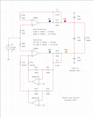
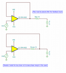
• I see from another thread that minimum Riso for the 1612/2211 family is 3R16, and the 1622 input capacitance is super low, so the 40R2 ballast resistors are total overkill. But they're there in case the better choice is an OPA1612, In which case I would need to inject a servo voltage using a 2K Rinj. And it doesn't hurt to put a little equal Rs on all ports of the 1622.

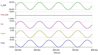
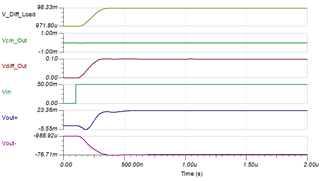
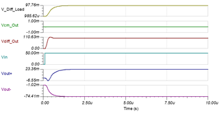
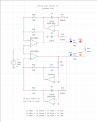
• The inverting side of the 1622 is for sure loaded to the hilt when driving a 600Ω external termination. But I see from the data sheet that it can push 66.6mA cleanly at the next lowest documented headphone load, so I'm wondering what happens at 28dBu differential with one side at ~64mA (phase margin, THD, et al). AFAICT it'll do 25dBu just fine.

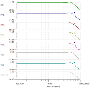
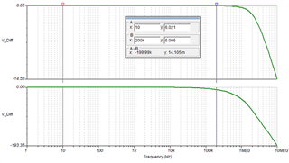
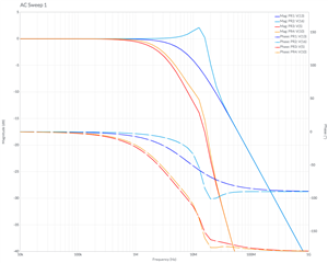
• There is no appreciable HF difference between this and a 10K load at the end of that football field of cable length.

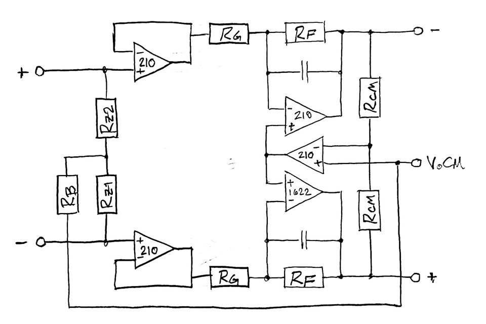
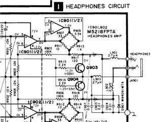
• No output protection drawn, but imagine the typical BAV99s from outputs to rails, and the 20R in the non-inverting 1622s FB loop is a good thing too.

Cheers.

  • Y'know, I thought I couldn't add a buffer because peaking, but it turns out I can. Which is a big deal for OPA1622 behavior -- now neither are loaded. And modeling the input capacitance helped too, in a way -- my inverting curve looks more like the Av=-1 curve on the data sheet. 0.8dB hump at 12.5MHz, or 0.3dB around 10MHz if I change the 1k5s to 1k2s (which it seems is not out of the ordinary). Adding even 10M of twisted pair at the back end wipes that away.

    Whaddayathink -- is this the real life, or is this just fantasy?

    Thanks

  • Hey Jonah,. 

    Interesting circuit! I put both circuits into Tina for analysis and to discuss. As a first pass I see that the 10 pF on the inverting node of the OPA1612 is causing some gain peaking at high frequencies due to the delay it is causing on the amplifier. If I remove this capacitor C1, the peaking is reduced. I also did a crude step response check on nodes PR1- 5 to check for ringing with a 10 mV step. PR5 of course has the most ringing due to the capacitance hanging off of the inverting terminal. Anyway, this was just a first pass to take a look at the circuit. I'll spend some more time with it to see if I can make some suggestions. Also let me know if you observe anything interesting and we can iterate on the design. 

    I also performed a DC analysis and the DC looks good. It converges fast so that is a good sign. 

    OPA1622 Line Driver V2.TSC

    Best Regards, 

    Chris Featherstone

  • Hey, it's (kind of) reality! With really great decoupling and layout obv.

    I should have stated clearly that the 10p hanging off of the inverter's divider is just there to model OPA1612 input capacitance. It's the *opposite* of what we want here. And R13 should be 20Ω.

    C12-C14 can safely be assumed to be anywhere from 330p to 3.3n in common use. R16 could be 600Ω, or (much) more commonly 10K to 100K. I can't find a good reason to differentially terminate the output before the LR pairs, but if so it would be normal to throw 100K in there.

    There is plenty of debate about advantages and disadvantages of the LR vs just more Riso. I figure 5.1Ω is more than safe for the 1622, and one could mess around with values of R17/R18 (up to 51Ω) if the inductors were to go away. But that's all in the realm of general driver output stability vs Cload, and the 1622 is already leagues above the 5532 or 4562 or 1678 or 1692 in that regard.

    Okay, so looking at your work, U3 looks stable. Is there some sort of "gotcha" there with common trace length and routing, or does R13 pretty much take care of Cload concerns? Normal R9/R12 common placement right at the -in should avoid adding any input capacitance. I'm just trying to think about anything I might be missing, because...uh...a low hanging fruit that's still on the tree might be there because no one else wanted to pick it.

    One of the things that gave me pause is that you can't AC couple the feedback loop at the U4 input...not that it's necessary to do so, I was just curious. Instant to-the-rails. I am not sure why one has to DC couple U4 if U3 provides bias to U2, but oh well.

    Shall I draw up a servo for this?

  • Hi Jonah,

    I would like to understand this better - I'm not familiar with the inductor/resistor in parallel (is that what you are calling the LR pair)?  Is the goal to minimize Riso?

    The additional amp. on the lower half will certainly add common-mode noise/distortion, an FDA would be much better suited... I know you know our FDAs very well, why are you looking to avoid an FDA?

    Regards,
    Mike

  • the inductor/resistor in parallel is a traditional (read: DOAs and transformers) way of ensuring that bandwidth doesn't collapse under heavy Cload / long cabling. the caveat is the hump somewhere in the mid-six figures, depending on values used. see Jensen AN-001, page 3. and yes, minimizing Riso is beneficial for avoiding loss into 600Ω -- I'm not a huge fan of ye olde 100Ω/600Ω attenuator as an output, which is what 2x 50Ω Riso becomes.

    re: avoiding an FDA

    the typical SE-to-diff output approach in pro audio, for lowest noise, is a buffer followed by an inverter. that or a DRV or THAT integrated solution, but neither are as low noise as the buffer/inverter. an FDA to go from SE -2dBu nominal to diff +4dBu nominal has a noise gain of 3, on both sides. a buffer and inverter that does the job has a noise gain of 2, but only on the inverter side, so when you sum them with a diff amp on the receiving end, it's less (I forget, probably 3.5dB noise). 

    now, look at the phase correlation between the buffer and inverter. the inverter is half as fast, assuming a dual. it also follows the buffer, so it's even slower than that. okay, do the natural thing -- put the buffer and inverter in parallel. phase is better, but still misaligned. i'm not splitting hairs at 10MHz here, it's a difference that is measurable all the way down to 10kHz. which is why people like fast amps for output.

    now, take that minor difference in phase of buffer and inverter and multiply it times several iterations of send/receive in a normal mix procedure in a normal transformerless audio console. things start getting pretty skewed.

    so, how do you A) keep it low noise, and B) retain phase relationship? well, ideally, you would use an amp for the inverter that's twice as fast as the buffer. that's not realistic at scale, because nobody makes a dual with one fast amp and one slow amp. so you would have to find singles that have the same amount of oomph, Cload stability, et al, but different speeds.

    thus...enter the circuit i am proposing. two buffers, with whatever it takes in one of their feedback loops to keep 'em aligned out to at least 200kHz, which is generally what we care about ("0.1dB variation from 10Hz to 200kHz" is a common claim these days). there are other ways, but all involve more than one stage, and mixing amp types.

    but, to your point, and a good one:

    what is THD+N like at the output of U1 here, vs U2? how much of that is common mode, and thus cancelable? and how much of that can we ameliorate if we add another buffer and inverter in the feedback loop, summing with 40R2 ballast resistors? it would afford us the noise freedom to keep increasing R9 and R12, with 2K being ideal. but is U3 (and U5 for that matter, if added) stable with R9 and R12 set to 2K? i'm going to guess no, but hey, worth a shot.

    probably the best price / performance balance here is to stick to the two duals, but see how low R9 and R12 can go before the U3 output starts looking more like the "into 600Ω" trace on the data sheet than the "into 2KΩ" trace on the data sheet. i'm willing to bet it's 1k2. OTOH, while the 1611/211 is unquestionably the best amp to use as U3, there is probably a better amp to use as U4 to keep HF distortion down. I suppose it would be worth dropping OPA828 into the U4 position just to take a look, as its speed is key here but its 4nV/rtHz noise isn't such a big deal as a buffer. three packages, all spendy, but maybe very high performing.

  • Hi Jonah,

    Ok, it makes sense on the inductors, but I would add that we do have other stabilization techniques that are not just using Riso that won't use a bulky inductor. But that's a good technique when writing an app. note about inductors!  There's no linearity impact?  Seems like that whole hysteretic B/H curve can cause problems but I don't have any data to support.

    We are wrapping up an app. note that describes a method for picking the optimal Riso, many times people over-compensate and use too much (it is the conservative approach, after all).  I'll let you know when Zach finishes that.

    Regarding the differential stage, we also have a few different techniques that are symmetrical on both sides.  You are probably aware but we'll post one of them just for documentation's sake.

    Regards,
    Mike

  • Sure, sounds good.

    I didn’t put a ton of time into the output. Could probably nix the inductors and just go with the resistors.

    I should probably post this for context, it’s an example of a multi-stage approach that accomplishes the phase alignment and no-load-on-the-preceding-stage goals. Noise should be competitive with the 1622/1612 approach we’re discussing, even with the increased HF noise of the 2210. And it’s cheaper. And just 10.2mA Iq. Comparable offset, but almost totally cancelable at the receiver.

    There could maybe be some current limiting around the 1622s…minimum stuff drawn for clarity. The 4 Rs are also a quad, like the Risos. This line driver goes at the back end of a 7Vrms single ended system and puts out 14Vrms into 600 or 10K. 

    Sidenote: If it were a 5Vrms/10Vrms system, the first 1622 half could be a NIC instead of a series buffer, without running into headroom issues. 

  • Hey Jonah, 

    I put together a simulation for stability. So far I have it for U2. It isn't perfect since the loop is broken and I didn't use the method of putting the input caps back in. However it is fairly close to the closed loop response I got in the prior simulation. I figured the input cap of the OPA1622 is low enough however this is one improvement in the analysis I could make. I have attached it below if you find it helpful. 

    Stability OPA1622 Line Driver V2.TSC

    Best Regards, 

    Chris Featherstone

  • You're saying that open loop gain and phase are doing what they're supposed to, yes?

  • Hey Jonah, 

    We can use it to monitor the phase with various Riso's to ensure stability when Aol and 1/beta meet. Or Acl is -3 dB. 

    Best Regards, 

    Chris Featherstone

  • We have reached the limits of my knowledge in this arena, so I will watch and learn. I would be varying in-loop Riso, post-loop Riso, and cable length right now if I had a PC! After disconnecting the inductors, of course.

  • Hi Jonah,

    You are correct that the 2-amp FDA circuit (buffer and inverter) produces group delays between the differential outputs. That approach is discussed in this article: https://www.ti.com/lit/an/sbaa265/sbaa265.pdf?ts=1683241933591&ref_url=https%253A%252F%252Fwww.google.com%252F 

    I've played around with similar ideas to produce a low-noise differential output with a fixed common-mode that does not introduce phase shifts between the output pins. My approach was a 3-amp FDA with a high-impedance differential input stage. Essentially, this is a discrete fully-differential instrumentation amplifier that can be used for low-voltage audio. In your case the input is 7Vrms and the output is 14Vrms, so 36V amplifiers can be used. It looks like you are considering OPA210 and OPA1622, these are great low-noise devices for this application. While I designed this circuit for a fully-differential input, it can be connected to a single-ended input as well.

    Here is the TINA simulation for my design:

    splitsupply_DIscrete FDA.TSC

    The gain is very flat over frequency with no gain peaking.

    The outputs are in phase with each other

    What is the minimum and maximum load capacitance you are expecting? I see some schematics show 1nF and some show 10nF. 

    OPA1622 has a very low output impedance and does not require much isolation resistance to drive heavy capacitive loads. 10Ω isolation resistors show very good settling behavior at the load for both 1nF and 10nF.

    capacitive load: 1nF common, 1nF differential

    capacitive load: 10nF common, 10nF differential

    A simpler approach would use the dual OPA2210 for the high-impedance buffer/gain stage and the fully-differential OPA1637 for the output stage. However, the OPA1637 would likely require a higher isolation resistance which would increase your error when connected to 600Ω load.

  • Hi Jonah,

    One quick correction, when I say the outputs are "in phase" with each other, I mean that the outputs are (near) perfect phase inversions as is expected for a differential output. This design does not exhibit the large group delays that occur in the 2-amp FDA design.

    Also, I just saw your comments on "in-loop" Riso vs "post-loop" Riso. I would like to clarify what you mean by this as Riso is always placed outside of the loop.

    OPA1622 has a very low output impedance which makes it very good at driving capacitive loads. Placing a series resistor in the loop as shown above only increases the total equivalent output impedance of the amplifier which will make it worse at driving a capacitive load. For certain amplifiers with complex output impedance, the in-loop resistor can be used to "flatten" the output impedance over frequency, that is to make the output impedance behave resistive instead of inductive. That is not necessary in this case as the OPA1622 already has a flat (resistive) output impedance for the frequencies of interest.

    Thanks,

    Zach

  • Chris / Zach -

    I played with this a bit and learned why people do what they do. 10R outside of the loop, sans inductors, provides the best bandwidth regardless of cable length. There is no advantage to putting Riso inside the loop. (Zach, Google "Doug Self" and "zero impedance output" for why I was doing that, and thanks for clarifying why it's unnecessary.) Maximum cable length that anyone would realistically use here is 150ft or 45M. There are occasions where people might use this for just 1M of cable, in which case you wouldn't get any substantial damping of the peak that the OPA1612 leaves at the output of the inverting OPA1622. But at 2dB, I'm guessing it's a non-issue. Typical cabling will always be 3M or more, and the peak is gone after 10M of cable.

    It appears that I have "sped up" the inverting OPA1622 in my circuit. It always has a wider passband than the non-inverting OPA1622, until the 2-pole response of the feedback loop kicks in. Am I thinking about this right? I'm sort of porting my understanding of composite amps over to this, where the slow amp is wrapped around the fast amp and the gain of both combine to make wider BW.

    I changed all the buildout resistances to 10R after realizing that servo'ing the 1622 would require more buildout resistance, and the application of loads to the inputs, and potentially more than two additional amplifiers. So I guess that one would just add a little DC injection point at the +in of the inverting OPA1612, and feed it with a divided-down output of a trimmer between the rails, as in so many Walt Jung examples and old school data sheets. I'm not exactly contracting for NASA, so wild temperature swings aren't so much of a concern.

    Zach, Wouldn't it be simpler to just put the entire output amp within the CM amp's feedback loop, like this?

    (whoops, output amps should both be labeled 1622)

    Maybe I’m missing some of the goals of your circuit, but this does what an FDA does, depending on how you treat VoCM. 

    Does the group delay of U4 + U2 + U1 = the group delay of U4 + U5?

    What are the values of the common mode sample resistors in the 1632, 1633, and 1637? I remember seeing 6K somewhere once, but was unable to find that again. Also does anyone know the input capacitance of the LM4562 or LME49860 offhand? It's not in either data sheet. I know there is an LMP version too but I can't remember the part number.

    There is another thread here in which Luis did some additional testing to extend the THP210/OPA1637 output specs beyond the data sheet, and sure enough, it will do the same levels as the 210, with a higher noise floor of course. Heck, it'll even do 20Vrms before it really takes off. I think that was just into a 2K load -- I don't expect to be able to give it lowish Rf values and still expect it to drive 600Ω. That's a job for the 1633, especially since it's priced right. Or, y’know, a 1622 and a 210.

  • I dunno why that ^ became a child post. Maybe a moderator could correct it, it appears when i make an edit i get a double post and have to delete the first.

    Chris, I reviewed the 828, and it seems to be the better amp for the buffer position in the feedback loop. And if the 211 is *actually* 45MHz and the 1611 actually 40MHz, then the 211 would be the clear choice for the inverter. LMK what you think. 

  • Hi Jonah,

    You are correct, both of the output amps should be OPA1622. I corrected this in the image below. In this configuration, both signal paths are symmetrical so there should be no phase lag issues at the output.

    There are a couple things about the FDA circuit you drew up that I believe make it a suboptimal solution compared to the design I recommended.

    1.) Your inputs are not necessarily high impedance, because they are connected through some resistors to your Vocm voltage source. In this configuration, your input signal and Vocm voltage may be affected by the resistor values chosen, the output impedance of the previous stage, the output impedance of your Vocm voltage source, and the voltage differential between Vocm and Vicm. The worst case is when connected in a single-ended configuration because your input-common mode voltage changes with the input voltage. This configuration would be recommended if the input is AC coupled, however with DC coupling as shown, the resistor networks will produce unwanted attenuation.

    2.) The lowest noise solution will apply the gain in the first stage. I believe you are only using a gain of 2V/V so this may not be a catastrophic difference. However it seems like you are interested in the lowest possible noise solution so I thought it would be worth mentioning. You could always simulate both circuits' noise performance in TINA-TI to see if you are ok with this tradeoff. 

    Zach, Wouldn't it be simpler to just put the entire output amp within the CM amp's feedback loop, like this?

    I considered this initially, but I noticed stability issues in the error amplifier's feedback loop when connecting it as shown in your circuit. This may be due to the phase shift introduced by the output amplifiers. I have also experimented with connecting the loop through a feedback compensation capacitor and this seems to work well. I haven't fully evaluated this so I'm not 100% sure which approach is best, however there does need to be some additional feedback for stability, likely a capacitor as shown below.

    Have a great weekend.

    Thanks,

    Zach

  • I’m glad someone has sim’d my 3-amp FDA, thanks for the heads up about stability. You drew me an output and I drew you an input, ie presumed to be unity or attenuating. Different story!

    I see your point about early gain. I had to spin your input amps around in my head so that they look like a differential gain stage in a mic preamp.

    You have VoCM tied to midsupply here, but i’m guessing it can tie to the receiver’s midsupply or ground, or an ADC common mode output, hence one of the reasons for separating VoCM & ViCM.

    I am unsure of the purpose of R28, R11, R12. Aren’t you trying to eliminate reliance on the sending unit’s ground? Is R28 a fail safe for in case someone blows the VoCM amp? And if you have to have R11 & R12 (which I guess you do because you’re not doing any DC removal), why aren’t they 500R each?

    The cap in the feedback loop is also confusing for me, but maybe if i stop thinking about a 350p/5K HPF i will get it. / edit: you’re integrating below 90kHz?

  • Had to unlearn and relearn a few things over the weekend...

  • Hi Jonah,

    Yes, purpose of the separate Vocm input is to drive the output to any common-mode using the error amplifier loop (U3).

    You are also correct that R11, R12, and R28 are for protection. R28 provides a DC current path to ground to ensure the loop is biased on startup and can discharge safely during shutdown. R11 and R12 provide a current limit for the input pins of the OPA1622.I designed this with a single 5V power supply in mind, so 5V/1kΩ = 5mA. The abs max rating for input pins is 10mA so the input is protected. For a higher power supply you could increase the resistor values for further current limiting. The non-inverting input is high-impedance so there is no voltage drop to be concerned with, although the higher resistance adds some additional noise of course. In practice I'm not sure how necessary this current limit will be, as these input pins are not directly connected to external sources. Since I am planning on experimenting with the error amplifier loop, and I have some concerns with stability, I decided to include these to make sure my OPA1622 is protected at all times.

    The cap in the feedback loop is an open circuit at DC, so it looks like it is running open-loop just like your drawing. At higher frequency (~90kHz) it begins to become a short just like in the original circuit I posted. This is somewhat of a simplification, but essentially it allows the proper DC biasing of the circuit for Vocm while providing loop stability at AC. The 90kHz is not a strict frequency requirement and this can be adjusted by changing the feedback capacitance. Eventually I plan on experimenting with this in a real circuit to determine the optimal solution. Perhaps you will try this in your design and let me know the answer Slight smile

    Regards,

    Zach

  • THS4031 is not the right amp for this because its BW shrinks dramatically with large signals, even with an Rf of 1KΩ. I'm using 20Vpp as a reference point because it is common on the high speed data sheets, and it is the maximum operating level of my general purpose amp, the OPA210. I posted this thread in the amplifiers forum to figure out a suitable replacement.

  • Hey Jonah, 

    Cool, it looks like Michael is helping out with that device. Hopefully that device will work out well in your application. 

    Best Regards, 

    Chris Featherstone

  • Thanks for the help! I’ll take a look at the xDSL line driver selection.

  • Chris, Zach -

    I'm back from looking at high speed amps, less than enthused at cost / Iq / Vos. Which is OK, because I figured out a way to do it with an OPA1602. There is no peaking and phase is aligned out to 800kHz. Huzzah.

    You'll see why the Rf and Rg are so low in a moment. I was looking into negative resistors, trying to figure out a way to negate the current drawn by the inverter. The classic current NIC operates at a gain of 2, which would overload the NIC if the amp it's relieving is already operating at a healthy maximum. But I was reminded of the Technics headphone amp section of a Groner composite thread on DIY Audio, wherein schematics show a current NIC that is being operated as a differential amplifier. They all look basically like this and use 741 equivalents:

    So I designed a unity gain NIC using the other half of the OPA1602 (pushing 23.4mA), and it doesn’t affect the bandwidth of the driver because bootstrapping, but I don't have a way of telling whether it effectively relieves the 680Ω total load that its own inverting input and the feedback inverter place upon the inverting OPA1622.

    Thanks for taking a look.

  • Hi Jonah,

    We'll need a few days to get back to you on this.

    Regards,
    Mike

  • Thanks Mike!

    FWIW in sim: the inverting 1622’s LPF could easily be something more like 100R/47p, and it is not crucial that all the Rs match. 68R/68p works too.