This thread has been locked.

If you have a related question, please click the "Ask a related question" button in the top right corner. The newly created question will be automatically linked to this question.

PCM3168A: PCM3168 TDM8 slave mode 96K output noise

Part Number: PCM3168A
Other Parts Discussed in Thread: PCM3168

Dear

 PCM3168A is configured as a TDM8 output, and the LRCKAD and LRCKDA are combined to connect to the LRCK of the main control chip

After BCKAD and BCKDA are merged, BCKAD is connected to BCK=12.288M of the main control chip, SPI mode of the main control, PCM3168 as slave, sampling rate LRCK:48K MCLK: 12.88M, BCK: 12.288M;

addr=42, val=0

addr=43, val=0

addr=44, val=0

addr=45, val=0

addr=46, val=0

addr=47, val=ff

addr=48, val=ff

addr=49, val=ff

addr=4a, val=ff

addr=4b, val=ff

addr=4c, val=ff

addr=4d, val=ff

addr=4e, val=ff

addr=4f, val=ff

addr=50, val=1

addr=51, val=6

addr=52, val=0

addr=53, val=0

addr=54, val=0

addr=55, val=0

addr=56, val=0

addr=57, val=0

addr=58, val=d7

addr=59, val=d7

addr=5a, val=d7

addr=5b, val=d7

addr=5c, val=d7

addr=5d, val=d7

addr=5e, val=d7

---readback---:

addr=c0, val=c0

addr=c1, val=6

addr=c2, val=0

addr=c3, val=0

addr=c4, val=0

addr=c5, val=ff

addr=c6, val=0

addr=c7, val=ff

addr=c8, val=ff

addr=c9, val=ff

addr=ca, val=ff

addr=cb, val=ff

addr=cc, val=ff

addr=cd, val=ff

addr=ce, val=ff

addr=cf, val=ff

addr=d0, val=1

addr=d1, val=6

addr=d2, val=0

addr=d3, val=0

addr=d4, val=0

addr=d5, val=0

addr=d6, val=0

addr=d7, val=0

addr=d8, val=d7

addr=d9, val=d7

addr=da, val=d7

addr=db, val=d7

addr=dc, val=d7

addr=dd, val=d7

addr=de, val=d7

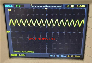
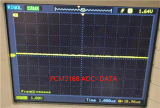
The output of 48K slave mode of TDM8 is normal. After the sampling rate is 96K, the output of single rate, double rate and automatic rate is abnormal. Please help to check the configuration of the 96K which needs to be changed, thank you! When configured in dua rate or auto mode, ADC DATA does not generate waveform; when configured in single rate, there is noise

  • Hello Liu,

    Thank you for reaching out. Please allow me some time to review these settings. In the mean time I have two questions.

    1. Please confirm. Does MCLK = BCLK? 
    2. What is register 41 set to?
  • hi andrew ,  

    Thank you for your reply,    1) MCLK=BCLK=12.288M;   2) reg=41, val=6     thanks! 

  • Hello Liu,

    When reviewing the registers above I have noticed the following:

    1. Register addr=45, val=0 #no flags
      1. The readback addr=c5, val=ff means that these All DACs (DAC1:8) have triggered zero input detected flags (See 9.3.9 Zero Flag for details on this feature). This suggests that inputs to the DACs are zero. This could be zero signal on the ADC or the result of clock errors.
      • After the sampling rate is 96K, the output of single rate, double rate and automatic rate is abnormal.
      1. Faster sampling rates only work in certain modes and clk frequencies. (See 9.3.4 System Clock Input and 9.3.5 Sampling Mode). The Table below shows that 96k is only supported in dual rate. Also, only the DAC side supports a 12.288MHz CLK. ADC performance would require a clock that is two times faster (24.5760MHz) to operate at 96k .

    Let me know if this helps.

    Best,
    Andrew

  • hi andrew ,  

    Thank you for your reply, 

    1) Register addr=45, val=0 #no flags,  reply  :This is because no signal comes out from ADC, so no signal is sent to DAC, indicating that 0 is detected

    2) Current configuration

    MCLK=BCLK=24.5M ,addr=40, val= c2.addr =50, val=2 are all set to dual-rate mode .The problem now is that the clock is working properly, that is, the ADC has no data output, and the ADC is always low  ,See Waveform and log information

    .PCM3168 Init...
    .write:
    .addr=40, val=c2
    .addr=41, val=6
    .addr=42, val=0
    .addr=43, val=0
    .addr=44, val=0
    .addr=45, val=0
    .addr=46, val=0
    .addr=47, val=ff
    .addr=48, val=ff
    .addr=49, val=ff
    .addr=4a, val=ff
    .addr=4b, val=ff
    .addr=4c, val=ff
    .addr=4d, val=ff
    .addr=4e, val=ff
    .addr=4f, val=ff
    .addr=50, val=2
    .addr=51, val=6
    .addr=52, val=0
    .addr=53, val=0
    .addr=54, val=0
    .addr=55, val=0
    .addr=56, val=0
    .addr=57, val=0
    .addr=58, val=d7
    .addr=59, val=d7
    .addr=5a, val=d7
    .addr=5b, val=d7
    .addr=5c, val=d7
    .addr=5d, val=d7
    addr=5e, val=d7


    ---readback---:
    .addr=c0, val=c2
    .addr=c1, val=6
    .addr=c2, val=0
    .addr=c3, val=0
    .addr=c4, val=0
    .addr=c5, val=ff
    .addr=c6, val=0
    .addr=c7, val=ff
    .addr=c8, val=ff
    .addr=c9, val=ff
    .addr=ca, val=ff
    .addr=cb, val=ff
    .addr=cc, val=ff
    .addr=cd, val=ff
    .addr=ce, val=ff
    .addr=cf, val=ff
    .addr=d0, val=2
    .addr=d1, val=6
    .addr=d2, val=0
    .addr=d3, val=0
    .addr=d4, val=0
    .addr=d5, val=0
    .addr=d6, val=0
    .addr=d7, val=0
    .addr=d8, val=d7
    .addr=d9, val=d7
    .addr=da, val=d7
    addr=db, val=d7
    addr=dc, val=d7
    .addr=dd, val=d7
    .addr=de, val=d7
    .
    .---PCM3168 Init OK---!
    .
    .time2=344

    .

    .......i2sout underflow 476
    .uart_data_process......

    .datas in nvram
    .Please press 'ENTER to enter into console,then type 'help' for help
    [dsp] Init_DSP_Para OK

    [dsp] time=331

    .[dsp] in:0.000000, 0.000000, 0.000000, 0.000000
    .[dsp] out:0.000000, 0.000000, 0.000000, 0.000000

  • Hi Liu,

    If the master device is not providing valid BCLK to the PCM3168, then there will be no valid I2S output from the device. The BCLK needs to be a square wave from 0V - DVDD with a duty cycle of around 50%.

    Can you improve the clock input's quality? Also, what is your scope bandwidth?

    Best,
    Andrew

  •  hi  Andrew   It is 100MHz  bandwidth  ,You mean the BCLK clock is not like a square wave ?  Let me retest bclk ,  Is there a problem with the register configuration  ?

  • Liu,

    A 100MHz Bandwidth scope is good. I was checking to see of it was a scope limitation. Causing a bad BCLK wave form (Please check the frequency rating of your scope probes as well). 

    The register configuration look okay. The capture from your previous post, however, shows BCLK as a 'triangle' shape. It also looks like this waveform goes from 1V-2V and this is not a valid BCLK. This means that there is either an issue with BCLK or the scope (or probes) is not acquiring the signal correctly).

    Making sure BCLK is a square wave that goes from 0V to the DVDD rail is the next step in the debug process.

    Best,
    Andrew

  • Thank you. I tried to put  sure BCLK is a square wave

  • Hi Liu,

    Did this solve your problem? If it did please let me know so I can resolve this post. If this did not solve your problem then provide more details to I can better help your issue. 

    Best,
    Andrew

  • Hi

    Clock is generated by DSP, bclk waveform has not been able to change into square wave, but I use AD1939 can work,  It is PCM3168 compatibility problem?

  • Hi Liu,

    PCM3168 does not have a compatibility issue. To understand what is happening in your application we first need to ensure that the BCLK is valid.

    Currently, the BCLK given to the device is not a valid wave form since it does not go low (to 0V). Data will not output without a BCLK. Please provide the PCM3168 with a BCLK that actually provides a logic high and a logic low, then we can proceed with the debug process.

    Best,
    Andrew

  •    Could you  help review the sch ? thanks!

  • Hi Liu, 

    I see no immediate issues with the schematic. Do you have any results from applying a valid bit clock?

    Best,
    Andrw

  • hi   Andrew

    The clock is generated by DSP , I   cannot   to changed. Why is  the 48K TDM8 OK?

  • Hi Liu,

    If I had to guess, the DSP is able to provide a valid BCLK when operating at 48k. To confirm this please capture wave forms (like the ones above) of the clocks at 48k sample rate. 

    Best,
    Andrew

  • Hello again Liu,

    Before following my previous post please see the below datasheet table. s

    From my understanding, your desired setting should be as follows: 

    • LRCLK = 96kHz
    • SCKI (MCLK):
      • MCLK_DAC = MCLK_ADC => 256*96k = 24.576MHz
    • BCLK = 128*96k = 12.288MHz

    Based on your screen shot in previous posts it looks like the BCLK is ~24MHz which would be too fast for this configuration. However, the SCKI (MCLK) input still needs to be 24.576MHz. 

    I apologize if this was misleading in previous posts, I should have clarified earlier. 

    Best,
    Andrew

  • Hi Andrew

       I know you mean,   DAC works in High speed mode and only needs one data, but ADC does not have high speed mode, so DIN 1\2 is needed for 96K, but my DSP does not have two data pins. Do you  any way to make ADC work in high speed mode ? only need a  data  wire  ?

  • Hi Liu,

    Highspeed mode is not available for the ADC. In order to operate both the ADC and the DAC on the same dateline then, the sample rate would have to be decreased to 48kHz.

    However, using two Data lines a 96k sample rate is possible. 

    Best,
    Andrew

  • thanks Andrew, 

    The DSP does not support the input of two data cables D0\D1 . thank you very much for your support.