Hi, TI support team
I am designing an AMP applied to a vehicle.
I have made inquiries through other inquiries, but I would like to ask further questions.
Currently, the product is designed as a TAS6422-Q1 product, and VBAT=14V, PVDD=20V (Boost converter).
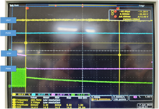
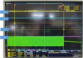
In the state that VBAT is Power on, when the boost converter is ON, PVDD=20V is applied, and when the boost converter is OFF, PVDD=14V (VBAT).
Even when the boost converter is OFF, voltage is output like input bypass. (This concept cannot be changed.)
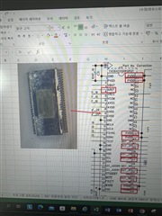
During the VESS AMP test after mounting on the vehicle under the above conditions, a burnt symptom occurred on the PVDD pins of the TAS6422-Q1 product (see the figure below).

The current power sequence is applied as follows.
Power ON : VBAT -> PVDD (approximately the same timing as VBAT) -> VDD
Power OFF: VDD -> VBAT, PVDD (PVDD gradually decreases from the boost voltage of 20V and becomes the same voltage as VBAT.)
VBAT and PVDD do not remove voltage even when Power is OFF.
Are there any parts that could fail under these conditions?
Is there a connection between the above mentioned bad situation and the power sequence?
If it is relevant, is there a way to compensate through software (register change)?
Thanks.
Regards,
MJ


