This thread has been locked.

If you have a related question, please click the "Ask a related question" button in the top right corner. The newly created question will be automatically linked to this question.

TAS6422-Q1: Inquiries about power sequence

Part Number: TAS6422-Q1

Hi, TI support team

I am designing an AMP applied to a vehicle.

I have made inquiries through other inquiries, but I would like to ask further questions.

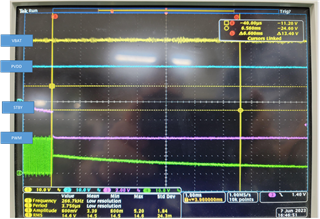
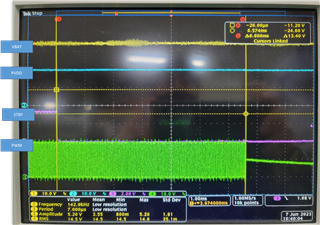
Currently, the product is designed as a TAS6422-Q1 product, and VBAT=14V, PVDD=20V (Boost converter).

In the state that VBAT is Power on, when the boost converter is ON, PVDD=20V is applied, and when the boost converter is OFF, PVDD=14V (VBAT).

Even when the boost converter is OFF, voltage is output like input bypass. (This concept cannot be changed.)

During the VESS AMP test after mounting on the vehicle under the above conditions, a burnt symptom occurred on the PVDD pins of the TAS6422-Q1 product (see the figure below).

The current power sequence is applied as follows.

Power ON : VBAT -> PVDD (approximately the same timing as VBAT) -> VDD

Power OFF: VDD -> VBAT, PVDD (PVDD gradually decreases from the boost voltage of 20V and becomes the same voltage as VBAT.)

VBAT and PVDD do not remove voltage even when Power is OFF.

Are there any parts that could fail under these conditions?

Is there a connection between the above mentioned bad situation and the power sequence?

If it is relevant, is there a way to compensate through software (register change)?

Thanks.

Regards,

MJ

  • MJ,

    Does the software use the /STDBY pin?  Good practice is to use the Standby Function before removing the DVDD (3.3V) power supply.

    We have tried many different power sequences and none of them cause a catastrophic failure.  As always, use the proper return path so this device can go through our QC department.

    Regards,
    Gregg Scott

  • Hi, Gregg

    Thank you for reply.

    We are using /STDBY.

    An additional question.

    Should PVDD become OV when STDBY OFF?

    As mentioned above, in my system, PVDD is applied at the same voltage as VBAT when STDBY is OFF.

    Is there any possibility that the product will be damaged in this situation?

    Thanks.

    Regards,

    MJ

  • MJ,

    The PVDD should never exceed the ABS Max value.  This should not be exceeded when on or off.  The product could be compromised if you exceed the ABS. Max value.

    Regards,
    Gregg Scott

  • Hi, Gregg

    This is not an inquiry related to ABS Max value.

    This is an inquiry about the status of PVDD being input when STDBY is low.

    Even when STDBY is low, PVDD is being applied at approximately 14V.

    Can these conditions damage the product?

    When STDBY=low, what state should PVDD be in?

    Thanks.

    Regards,

    MJ

  • Hi, Gregg

    The waveforms below are the two waveforms of the product designed by the customer.

    1) When the system is OFF, STDBY goes low and MCK turns off. Accordingly, the PWM is immediately turned off.

    Is PWM off right away a problem with the product?

    2) If only STDBY is changed to low in the System ON state, PWM comes out for a certain period of time as shown in the waveform below and then turns off.

    The above two waveforms and conditions are also confirmed to be the same for EVM.

    Can the two waveforms and conditions cause damage to the product?

    Thanks.

    Regards,

    MJ

  • MJ,

    Both of these scenarios will NOT damage the device.  There is no issue with the audio either.

    Regards,
    Gregg Scott

  • Dear, Gregg

    Please confirm the above question.

    Should I keep PVDD=0V when STDBY=Low?

    Currently, our circuit is maintained at 14V.

    Please confirm.

    Thanks.

    Regards,

    MJ

  • MJ,

    You do not need to force PVDD low when in standby.  It can be connected to the battery all the time.

    Regards,
    Gregg Scott