Hi ,
the TLV320ADC6120 is not assigning audio channel to designated slot using this code
// ********* ASI_CH1 channel 1
// bit 7-6 = 00 | Reserved write 00
// bit 5-0 = 000000 | 0d = TDM is slot 0 or I2S, LJ is left slot 0
// BIN = 00000000 HEX = 0x00
ADC_I2C_Write(ASI_CH1, 0x00);
// ********* ASI_CH2 channel 2
// bit 7-6 = 00 | Reserved write 00
// bit 5-0 = 000001 | 1d = 1d = TDM is slot 1 or I2S,
// BIN = 00000001 HEX = 0x01
ADC_I2C_Write(ASI_CH2, 0x01);
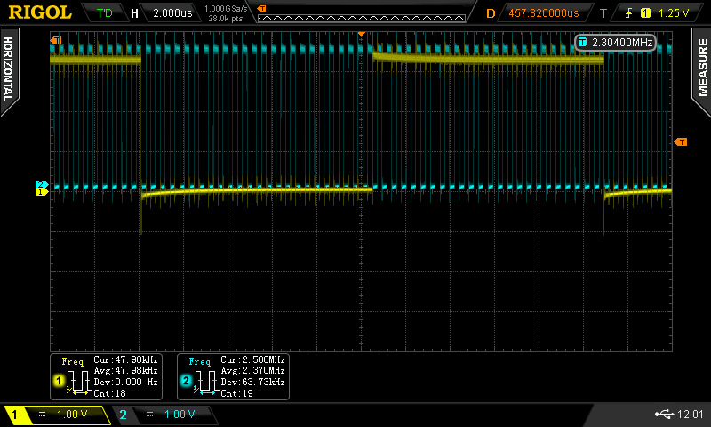
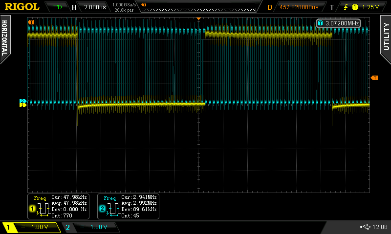
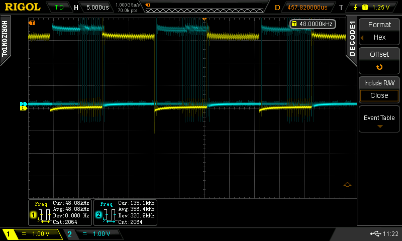
I believe something is wrong with the setup code only 1 slot in I2s mode is populated with SDO data from the ADC
here is FSYNC and ADC sdout.
audio samples in slot 0 , nothing in slot 1
I am using PLL in auto mode and device should be master. I2S 2 channel.
here is my setup code;
/********** POWER ON ADC ***************/
/* wait for power supply to settle */
osDelay(250u); /* 250ms. */
/* Power on ADC using MOSFET */
HARDWARE_adcPowerControl(TRUE);
/* wait for ADC to power up*/
osDelay(250u); /* 250ms. */
/* ######################## ADC TLV320ADC6120 SETUP ############################## */
// register pages
// Page 0x00 normal setup registers ,
// Page 0x01 VAD voice activity detection
// Page 0x02 Programmable Coefficient Registers:
// Page 0x03 Programmable Coefficient Registers:7 -12
// Page 0x04 Mixer Settings
/* go to page 0 */
ADC_I2C_Write(PAGE_CFG, 0x00);
// SW_RESET Register(Address = 0x1)[Reset = 0x0]
ADC_I2C_Write(SW_RESET, 0x01);
osDelay(20u); /* 10ms. */
/* go to page 0 */
ADC_I2C_Write(PAGE_CFG, 0x00);
// Wake-up device by I2C write into P0_R2 using internal AREG
// bit 7 = 1 | 1d = Internally generated 1.8 - V AREG supply using an on - chip regulator(use this setting when AVDD is 3.3 V)
// bits 6-5 = 00 | Reserved bits; Write only reset values 0
// bits 4-3 = 01 | 0d = VREF quick-charge duration of 3.5 ms (typical) | 3d = VREF quick-charge duration of 100 ms (typical)
// bit 2 = 0 | 0d = I2C broadcast mode disabled
// bit 1 = 0 | Reserved bit; Write 0
// bit 0 = 1 | 1d = Device is NOT in sleep mode
// BIN 10001001 HEX 0x81
ADC_I2C_Write(SLEEP_CFG, 0x81);
osDelay(1u); /* 1ms. */
// *********** GPIO_CFG0 Register ***************
// bit 7-4 = 1010 | 10d = GPIO1 is configured as a master clock input (MCLK)
// bit 3 = 0 | Reserved bit; write 0d
// bit 2-0 = 010 | 2d = Drive active low and weak high
// BIN 10100010 HEX = 0xA2
ADC_I2C_Write(GPIO_CFG0, 0xA2);
// ********* MST_CFG0 Register *************************
// bit 7 = 1 | 1d = Device is in master mode (both BCLK and FSYNC are generated from the device)
// bit 6 = 0 | 0d = Auto clock configuration is ENABLED
// bit 5 = 0 | 0d = PLL is enabled in auto clock configuration
// bit 4 = 0 | 0d = DO NOT Force gate BCLK and FSYNC when being transmitted from the device in master mode
// bit 3 = 0 | 0d = fS is a multiple (or submultiple) of 48 kHz
// bit 2-0 =111 | 7d = 24.576 MHz // 1d = 12.288 MHz MCLK_FREQ_SEL
// BIN = 10000001 HEX = 0x81 // auto clock config 12.288mhz oscilator
// BIN = 10000111 HEX = 0x87 // auto clock config 24.576mhz oscilator
ADC_I2C_Write(MST_CFG0, 0x81);
// ********* MST_CFG1 Register *************************
// bits 7-4 = 0100 | 4d = 44.1 kHz or 48 kHz FS_RATE Page 0
// bits 3-0 = 0011 | 4d = Ratio of 64 | 3d = Ratio of 48 :N BCLK clocks in FSYNC cycle
// BIN = 01000100 HEX = 0x44 64 bclks in fsync
// BIN = 01000011 HEX = 0x43 48 bclks in fsync
ADC_I2C_Write(MST_CFG1, 0x43);
/* go to page 0 */
// ADC_I2C_Write(PAGE_CFG, 0x00);
// ******** IN_CH_EN Register input channels config *******************
// bit 7 = 1 | 1d = Channel 1 is enabled
// bit 6 = 1 | 1d = Channel 2 is enabled
// bit 5 = 0 | 0d = Channel 3 is disabled
// bit 4 = 0 | 0d = Channel 4 is disabled
// bits 3-0 = 0000 | reserved write 0000d
// BIN = 11110000 HEX = 0xC0
ADC_I2C_Write(IN_CH_EN, 0xC0);
// ******** BIAS_CFG Register ****************************************
// 7 bit = 0 | reserved write 0
// 6-4 bits = 000 | 0d = Microphone bias is set to VREF (2.750 V, 2.500 V, or 1.375 V)
// 3-2 bit = 00 | reserved write 00
// 1-0 bits = 00 | 0d = VREF is set to 2.75 V to support 2 VRMS for the differential input or 1 VRMS for the single - ended input
// BIN = 00000000 HEX = 0x00
ADC_I2C_Write(BIAS_CFG, 0x00);
// CLK_SRC Register(Address = 0x16)
// bit 7 = 0 | 0d = 0d = BCLK is used as the audio root clock source
// bit 6 = 0 | 0d = 0d = MCLK frequency is based on the MCLK_FREQ_SEL (P0_R19) configuration
// bit 5-3 = 011 | 1d = 256 12.288mhz | 3d = Ratio of 512 ( 24.576mhz )
// bit 2 = 0 | reserved write 0
// bit 1 = 0 | 0d = Do not invert BCLK polarity for FSYNC generation
// bit 0 = 0 | reserved write 0.
// BIT 00011000 HEX = 0x18
// ADC_I2C_Write(CLK_SRC, 0x18); // PLL ENABLED in AUTO MODE , NO NEED TO WRITE THIS ?
// ******* ASI_CFG0 Register I2S Mode with 32 Bits/Channel SAI word
// bits 7-6 = 01 | 1d = I2S mode
// bits 5-4 = 10 | 3d = Output channel data word-length set to 32 bits | 2d = Output channel data word-length set to 24 bits
// bit 3 = 0 | 0d = FSYNK Default polarity as per standard protocol
// bit 2 = 0 | 0d = BCLK Default polarity as per standard protocol
// bit 1 = 0 | 0d = Default edge as per the protocol configuration setting in bit 2 (BCLK_POL)
// bit 0 = 0 | 0d = Always transmit 0 for unused cycles , use one for hi-Z
// BIN = 01110001 HEX = 0x70 // 32bit word
// BIN = 01100000 HEX = 0x60 // 24bit word
// BIN = 01000000 HEX = 0x40 // 16bit word
ADC_I2C_Write(ASI_CFG0, 0x60);
// ASI_CFG1 Register
// bit 7 = 0 | default 0d = Transmit the LSB for a full cycle
//bits 6-5 =00 | default 0d = Bus keeper is always disabled
//bits 4-0 = 00000 | 0d = ASI data MSB location has no offset and is as per standard protocol
// ADC_I2C_Write(ASI_CFG1, 0x00);
// ************* ASI_OUT_CH_EN Register **************
// bit 7 = 1 | 1d = Channel 1 output slot is enabled
// bit 6 = 1 | 1d = Channel 2 output slot is enabled
// bit 5 = 0 | 0d = Channel 3 output slot is disabled
// bit 4 = 0 | 0d = Channel 3 output slot is disabled
// bits 3-0 = 0000 | reserved write 0000
// BIN = 11000000 HEX = C0
ADC_I2C_Write(ASI_OUT_CH_EN, 0xC0);
// ********* ASI_CH1 channel 1
// bit 7-6 = 00 | Reserved write 00
// bit 5-0 = 000000 | 0d = TDM is slot 0 or I2S, LJ is left slot 0
// BIN = 00000000 HEX = 0x00
ADC_I2C_Write(ASI_CH1, 0x00);
// ********* ASI_CH2 channel 2
// bit 7-6 = 00 | Reserved write 00
// bit 5-0 = 000001 | 1d = 1d = TDM is slot 1 or I2S,
// BIN = 00000001 HEX = 0x01
ADC_I2C_Write(ASI_CH2, 0x01);
// **** CH1_CFG0 Register Field Descriptions
// bit 7 = 0 | 0d = Microphone input , 1d = Line input
// bits 6-5 = 01 | 1d = Analog single-ended input | 0d = Analog differential input
// bit 4 = 0 | 0d = AC-coupled input | 1d = DC-coupled input
// bits 3-2 = 0 | 0d = Typical 2.5-kΩ input impedance | 1d = Typical 10 - kΩ input impedance | 2d = Typical 20 - kΩ input impedance
// bit 1 = 0 | reserved write 0
// bit 0 = 0 | 0d = DRE / AGC / DRC disabled | 1d = DRE or AGC or DRC enabled based on the configuration of bit 3 in register 108 (P0_R108)
// BIN = 00100000 HEX = 0x20
ADC_I2C_Write(CH1_CFG0, 0x20);
// **** CH2_CFG0 Register Field Descriptions
// bit 7 = 0 | 0d = Microphone input
// bits 6-5 = 01 | 1d = Analog single-ended input | 0d = Analog differential input
// bit 4 = 0 | 0d = AC-coupled input | 1d = DC-coupled input
// bits 3-2 = 0 | 0d = Typical 2.5-kΩ input impedance | 1d = Typical 10 - kΩ input impedance | 2d = Typical 20 - kΩ input impedance
// bit 1 = 0 | reserved write 0
// bit 0 = 0 | 0d = DRE / AGC / DRC disabled | 1d = DRE or AGC or DRC enabled based on the configuration of bit 3 in register 108 (P0_R108)
// BIN = 00100000 HEX = 0x20
ADC_I2C_Write(CH2_CFG0, 0x20);
// CH1_CFG1 register
// bit 7 - 1 = 1010100 | 84d = Channel gain is set to 42 dB
// bit 0 = 0 | 0d = Positive sign channel gain
// BIN 10101000 HEX = 0xA8
ADC_I2C_Write(CH1_CFG1, 0xA8);
// CH2_CFG1 register
// bit 7 - 1 = 1010100 | 84d = Channel gain is set to 42 dB
// bit 0 = 0 | Channel-1 gain sign configuration.
// 0d = Positive sign channel gain
// BIN 10101000 HEX = 0xA8
ADC_I2C_Write(CH2_CFG1, 0xA8);
// ************ PWR_CFG Power up the ADC, MICBIAS PLL etc Register Field Descriptions *****************
// bit 7 = 1 | 1d = Power up MICBIAS
// bit 6 = 1 | 1d = Power up all enabled ADC and PDM channels
// bit 5 = 1 | 1d = Power up the PLL | 0d = Power OFF the PLL
// bit 4 = 0 | 0d = Channel power-up, power-down is not supported if any channel recording is on
// bits 3-2 = 00 | 0d = Channel 1 and channel 2 are used with dynamic channel power - up, power - down feature enabled
// bit 1 = 0 | 0d = VAD is disabled , Enable voice activity detection (VAD) algorithm
// bit 0 = 0 | reserved use 0
//
// BIN = 11100000 HEX = E0
ADC_I2C_Write(PWR_CFG, 0xE0); // 0xE0 power ON everything including PLL
// wait for adc to power up
osDelay(250u);