This thread has been locked.

If you have a related question, please click the "Ask a related question" button in the top right corner. The newly created question will be automatically linked to this question.

TPA6110A2: not working

Part Number: TPA6110A2
Other Parts Discussed in Thread: TPA6111A2

Hi, 

I'm trying to design a headphone amplifier based on the TPA6110A2.

This is my schematic:

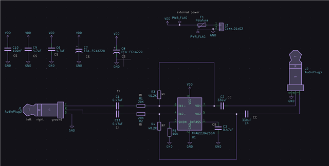
The audio plugs are actually jacks on the PCB.

I'm testing with a 3.3V power supply and with a 1cell Lithium Ion, with 4.2V max.

There is no output whatsoever.

I'm measuring the audio input signal on C1 and before R1, but after R1, at the junction with R3 I'm measuring 2V DC level.

On the other side, there's audio signal on C11 and before R2, but after R2, at the junction with R4 I'm measuring 1V DC level.

My bypass is not VDD/2, as I'm measuring around 500mV on CB (C3).

Power draw is 90mA at 3.3V while doing nothing, even with both audio connectors unplugged.

With the shutdown pulldown resistor in place I'm measuring around 800mV at the SHUTDOWN pin.

Such a simple design, yet I've clearly made a mistake somewhere. I've tried messing around with the gain resistors but to no luck.

I'm sorry, maybe I missed something, I would like some help please..

Thank you, 

  • Hi Secere,

    What type of capacitors are you using for C1, C2, C3, C4 and C11? Are all these ceramic?

    The low voltage on Bypass pin, along with relatively high current regardless if the device is enabled or not, are not OK. If you test by removing input, output and bypass caps, do you see any change on bypass voltage?

    Best regards,
    -Ivan Salazar
    Applications Engineer

  • Hi Ivan,

    Yes all bypass caps are ceramics. I only have 2 bulk electrolytics as bulk on the power input.

    I've removed, one by one, all parts on the PCB except the TPA itself and the pulldown resistor for the SHUTDOWN pin.

    I've strapped over the PTC fuse.

    Same high power consumption and same voltage level on the BYPASS pin. (<1V at 3.3V supply).

    I'll see if I have any other fresh TPA-s and try assembly one on a fresh PCB, going the other direction; assembly the PCB part by part and see what changes.

    The Exposed Pad can be connected to GND, correct? 

    I've seen another thread on the forum talking about this.

    At this point I think I might have a PCB manufacturing defect, even though I can't see anything wrong on the top and bottom layer at least and doing a continuity test on a bare PCB doesn't reveal anything wrong.

  • I've solved it myself Ivan, don't worry about it.

    Looks like I've ordered the wrong part.

    Board is designed for TPA6110 and I've assembled TPA6111 on it.

    What are the major differences between the two other than the footprint ? And what would you recommend ?

  • Hi Secere,

    Thanks for the updates. All TPA611x family are same just different in footprint options.
    You should just either replace the IC on your current PCB or update the PCB to match TPA6111A2.

    Best regards,
    -Ivan Salazar
    Applications Engineer