This thread has been locked.

If you have a related question, please click the "Ask a related question" button in the top right corner. The newly created question will be automatically linked to this question.

TAS2781EVM: Standard config for amplifier evaluation with resistive load and APx

Part Number: TAS2781EVM
Other Parts Discussed in Thread: PPC3-EVM-MB

Hello,

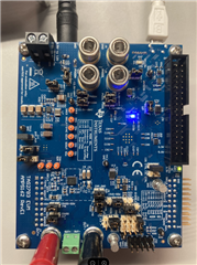
I am working on a new portable speaker that requires high efficiency. I purchased a TAS2781EVM for evaluation and am having significant issues with it. I have followed along on the quick start but am running into a few issues.

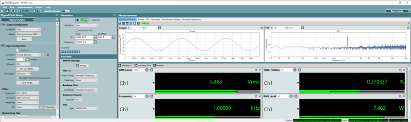
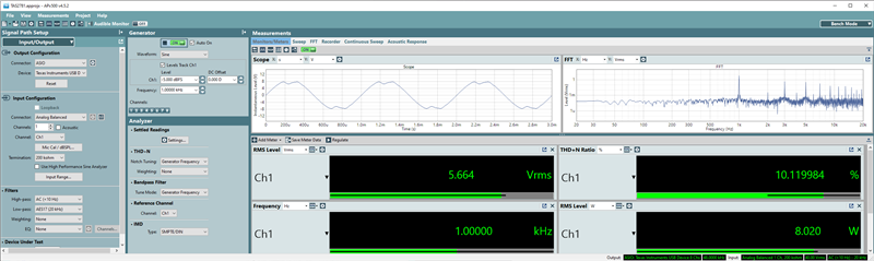
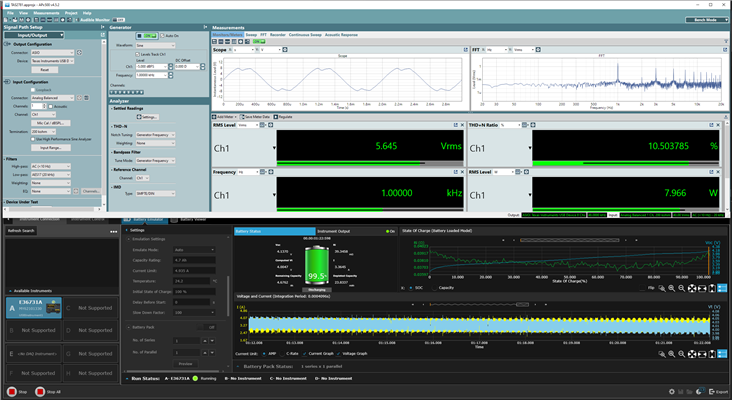
1. I am only able to get out a watt or so of power into a 4Ω dummy load. And pushing the input signal to 0dBFS is a guaranteed over current event as reported by the status registers.

   - Is this due to the smart speaker characterization?

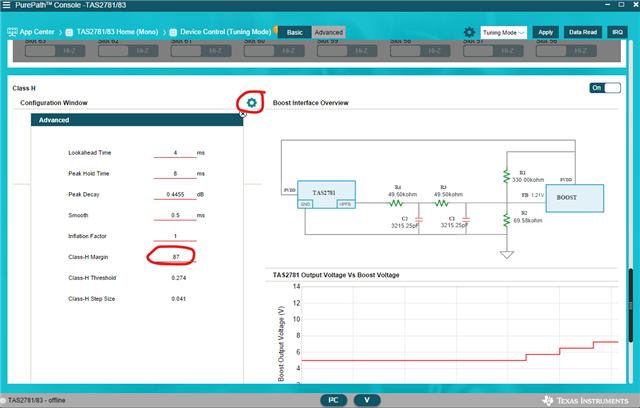
2. I am only seeing ~7V on the PVDDH supply. This is regardless of whether or not I enable Class-H operation and populate J14. I basically always have 7V.

  - The Schematics show that this should be 12v nominal, I have not gone in and measured the resistor values in the FB path, but I am assuming the EVM came in a properly configured state.

Before I spend a ton of time debugging what I was hoping to be a quick evaluation, is there a default configuration that should be used for evaluation? Would be really helpful if there was a starting point for this EVK that did not require a drive in an enclosure (does not yet exist). For evaluation I am looking for the following:

- Flat EQ 20Hz-20kHz

- No DRC

- 0dBFS in = 0dBFS out

- Stable into a 4Ω purely resistive load (maybe this is my issue)

- Class H operation and Y bridge enabled to run off of a 3.6V nominal Li-ion battery.

  • Hi Adam. 

    It seems like you are doing everything correct here, I can share with you a configuration that can accomplish what you need. regarding your questions and observations

    I am only able to get out a watt or so of power into a 4Ω dummy load. And pushing the input signal to 0dBFS is a guaranteed over current event as reported by the status registers.

    yes, this is due to incorrect characterization. if you are using a resistive load for evaluation it is recommended to put the device into "ROM Mode". ROM mode is the devices functional mode where all the smart amp functionality such as speaker protection, EQ, DRC etc. functionally ROM mode makes the device behave as a simple class-D amplifier. the smart amp protection will be getting incorrect feedback from the load and will be very conservative in limiting the output power. 

    Here is what you do to enable the Class-H and disabled the speaker protection

    - open new ppc3 file

    - go to "tuning and audio processing" panel

    - select a tuning option which includes the Class-H

    - go back and then select "device control" panel

    - scroll down and then enable the class-H panel

    - in top right of the window select the drop down menu which says "Tuning mode" change it to "Rom Mode" 

    - press apply

    after doing this the device will have smart amp disabled, and class-H should be enabled with Y-bridge

    alternatively you can use this .cfg file and run it in PPC3 using the "I2C" tool from the bottom of the window

    TAS2781_0x70_ClassH_Y-bridge_Enabled.cfg

    I am only seeing ~7V on the PVDDH supply. This is regardless of whether or not I enable Class-H operation and populate J14. I basically always have 7V.

    the EVM default voltage will be ~7V. when J14 is inserted the voltage should be ~5V. then with class-H enabled the device can modulate the boost up to ~12V.

    EVM Jumper settings

  • Arthur,

    Thank you for this. The Class H operation is working as expected. Both direct I2C via your cfg file and me manually executing these steps is working for me.

    I am seeing an issue as I approach -0dBFS. At -6dBFS in I have 5.46Vrms out and 0.28% THD+N. PVDDH is 9.39V and every thing looks good. As I then bump up the input to -5dBFS I see clipping and THD+N jumps to ~10%. PVDDH also bumps up to 10.4V which I believe is inline with what I should be seeing. 

    I am currently violating the test setup suggested by the datasheet and using a APx555 directly connected to the DUT via the balanced input. No DIFF-SE converter or AUX-0025 in the mix. Below is a screen shot of the waveform on the APx.

    Is this the added distortion that you would expect to see due to measurement parasitics influencing the feedback loop?

    Are you using an existing opamp EVK or something readily available for your instrumentation amplifier? If there is nothing available I will hack something together here.

    Finally I am hearing very loud PWM noise from the PCBA as I increase power. Is this standard, and are there recommendations for boost converters that pair well with this amplifier and do not cause significant noise?

    Thank you,

    Adam

    -6dBFS:

    -5dBFS:

  • Also note that I am using a Keysight E36731A battery emulator as the voltage source for this test.

    Vin ~4V

    Iin ~3.36A

    This PSU has a simulated output impedance of 39mΩ. And is trying to simulate a 4700mAh li-ion battery pack.

  • Hi Adam, 

    the increase THD you are seeing  is not due to AUX or D2S Filters. 

    It seems like there is some error in the boost voltage and the amplifiers output is prematurely clipping. you can adjust the Class-H Margin parameter slightly (lower it to ~0.8 or a bit more) to give the amplifier better headroom and prevent the clipping

    We do have one EVM that has the diff-se filter on it in the "PPC3-EVM-MB" but i would not ask you to purchase it. the diff-se filter will only improve the THD measurements by 2-3 dB, which can be important when we are advertising our performance in our data sheets, but for your evaluation the difference between 0.0001% THD and 0.0005% THD wont be critical, considering your speaker will be 0.5%-1% 

    the noise from the EVM We suspect is the piezoelectric effect of the MLCC caps. you can find some layout guides online which can give recommendations on how to best do the layout, the noise is not from the boost IC itself

    Regards,
    Arthur

  • Hello Arthur,

    Thank you for this. It is correct that I clipping the output rail. However, the problem appears to be that the boost converter on the EVK is only capable of 12.6V 2A. I am running into that limitation. I see the feedback pin drop below the 1.2V reference and PVDDH is hitting 12V. As I push into that clipping the rail begins to sag as it cannot provide ample current.

    I will look to wire in another boost converter for this.

    Thank you,

    Adam