This thread has been locked.

If you have a related question, please click the "Ask a related question" button in the top right corner. The newly created question will be automatically linked to this question.

TPA3004D2

Other Parts Discussed in Thread: TPA3004D2

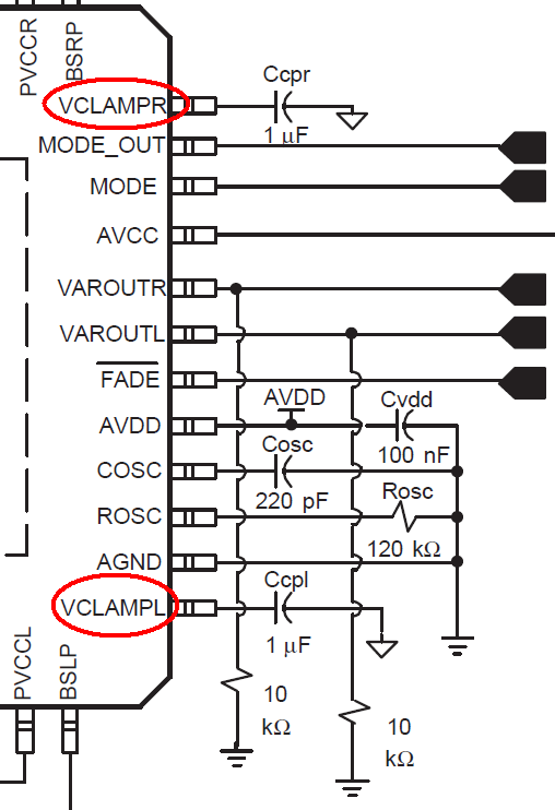
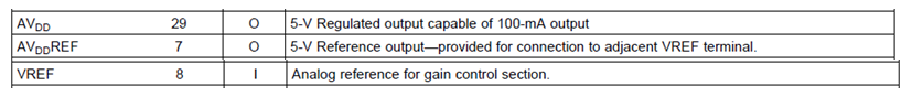
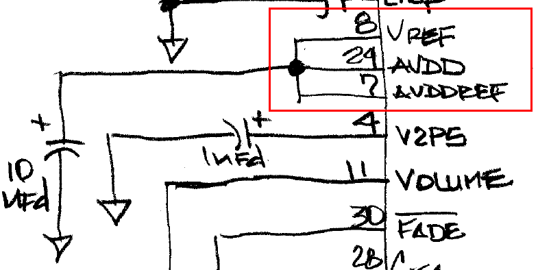
HELLO I WILL BE USING THIS DEVICE AS A FRONT END DEVICE FOR A HIGH VOLTAGE FULL BRIDGE LAYOUT I NEED TO SEE IF I CAN GET SOMEONE EMAIL ADDRESS SO I CAN SEND THEM A DRAWING OF HOW I HAVE THE PART LAID OUT TO SEE IF ITS OKAY ARE DO I NEED TO MAKE CHANGES TO THE LAYOUT

LET ME NO ASAP

IAM DESIGNING NOE AND I NEED TO GET THIS DONE

THANKS,

WILLIE L. MCCAIN

DRIECT EMAIL ADDRESS

wlmccain@mccainlaboratories.com

  • Hi Willie,

    What voltage are you using? The TPA3004D2 is relatively low voltage device (15V).If you need a high voltage device we have some that are better suited. Have you ordered the EVM (http://www.ti.com/tool/tpa3004d2evm) for the TPA3004D2? The Gerber files for our EVM can be found here: http://www.ti.com/litv/zip/sloc008 (EVM Gerber Files)

    If you follow the design of the EVM you should be okay. Good practice is it to keep the bootstrap caps (BSRP, BSRN, BSLP, and BSLR) and supply decoupling caps (Cs caps on datasheet) relatively close to the device, to reduce any parasitic inductance, which may cause some ringing.

    Best Regards,

    Jacob

  • okay you are correct i will be using this part as a front end device not the driver device

    this is why i ask for a email so i can send you a layout so you can see clearly what iam trying to do

    i need to just bias the part to get the drive signals at 15 vdc and they will go to the driver device for the high voltage 5040.TPA3004D2 LAYOUT.pdf

     TAKE A LOOK AND GET BACK PLEASE I JUS NEED TO NO IF THE PINS ARE CORRECT

    AGAIN THE PART WILL ONLY BE USED AS A FRONT END DEVICE FOR THE DRIVE SIGNALS

    THANKS,

    WILLIE

  • Hi Willie,

    From what I can see, you are using single ended inputs, is that correct?

    From the pinout you gave me I did see some areas that need some attention.

    1. Pins 36 (VCLAMPR) and 25 (VCLAMPL) should be connect to GND through a cap.

    2. Pins 8, 29, and 7 (Vref, AVDD, & AVDDref). I would try to do something more of the lines of the datasheet or EVM schematic.

    Like I said before, I would try to stick to something close to the EVM and/or datasheet. Our reference designs and EVMs are somethings that can be built upon and are excellent in aiding designs. I hope this helps.

    Best Regards and have a Happy New Year,

    Jacob