


Tool/software:
Hi everyone,
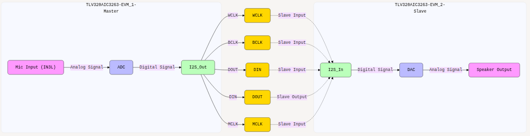
I'm working on a project where I connect two TLV320AIC3263EVM-U boards using the I²S bus.
After spending several days troubleshooting and experimenting, and with the help of valuable information shared by forum members, I was finally able to get my application working. Now I have a follow-up question regarding the MCLK (Master Clock) connection.
Question
In this thread, Luis mentions:
“All the devices would work at the same frequency.”
My question is:
-
Is it acceptable to use two separate crystals running at the same frequency for each board?
-
Since crystals may not oscillate at exactly the same frequency, would that small deviation cause synchronization issues?
-
Do we need to share the same MCLK source between devices to ensure perfect timing?
In my case, I did not share a single MCLK source between the two EVMs, and it still worked.
I also tested the setup by removing the JP49 jumper on the slave EVM and connecting its pin 2 to pin 2 of JP49 on the master EVM (configured for MCLK output via pins 2–3). This effectively shared the master’s MCLK between both boards using an external wire — and it worked without issues.
I’m wondering if this is reliable, or if it might cause subtle timing issues down the line.
 Setup Details
Since my previous topic was closed, I’m sharing the working setup and code here for future reference:
 Previous topic (with background):
 TLV320AIC3263EVM-U: Communicating Two EVMs via Mono PCM
 Connection Setup:
I removed J17, J18, J19, J20 jumpers on both boards and manually connected the middle pins (pin 2) as follows:
| Master Pin | Slave Pin |
|---|---|
| J17 → | J18 |
| J18 → | J17 |
| J19 → | J19 |
| J20 → | J20 |
This configuration allowed me to transmit and receive audio between the two EVMs successfully.
 Helpful Reference for Master Mode Configuration
I learned how to configure WCLK and BCLK output (setting the codec as I²S master) from this topic:
TLV320AIC3262: Configuration as Master Mode
Even though the issue described by Rizwan Chikodi appeared to be solved, the provided example didn’t work in my case — I got the same waveform on the scope (high 3.3V), which depends on JP50 jumper (3.3V vs 1.8V IOVDD selection).
The key solution was:
-
Setting the BCLK and WCLK dividers in:
Codec Control → Digital Settings → ASI Clockstab. -
And powering BCLK and WCLK div powers.
#audio serial interface routing configuration for ASI1
w 30 00 04
w 30 08 f0 # ASI1 Left and Right DAC mixed of Left and Right data
w 30 0a 24 # Master mode WCLK and BCLK output. (You may need to configure 1.8V / 3.3V data levels on EVM using JP50 jumper)

w 30 00 04
w 30 0c 84 # BCLK N divider powered up, N value is 4 => We need to send data: 32bit/1channel x 2channel x 48KHz = 3.072 MHz is required. 12.288MHz / 4 = 3.072 MHz.
w 30 0d a0 # ASI1 Primary WCLK divider N = 32 and powered up. Dont know why 32 gives us 48kHz. I expected to select 32x2=64 for WCLK=48kHz
w 30 01 18 # ASI1 Audio Interface = I2S, ASI1 Data Word length = 32 bits, DOUT1 will not be high impedance while ASI1 is active
 I²S Master Code: Bi-Directional Audio
With the setup below:
-
You can send microphone input from the slave device to the Class-D speaker on the master.
-
Simultaneously, you can send microphone input from the master to the Class-D speaker on the slave.
I will share the full working code and connection details to help others searching through the forum — since it was quite disappointing to find many unresolved topics during my own research.
Let me know if anyone has suggestions regarding the MCLK setup or notices any potential issues with using independent crystals.
Thanks again for the great support from the community!
EVM1: I2S Master Code (Both Send and Receive)
#######################################################
# Clock configuration
# -----------------------------------------------------
# - MCLK = 12.288MHz
# - FS = 48kHz
# - I2S Master
#######################################################


#######################################################
# FIFO Configuration
#######################################################
w 30 00 00 # Select Page 0
w 30 7f 78 # Select Book 120
w 30 32 80 # Enable DAC FIFO
w 30 7f 64 # Select Book 100
w 30 32 80 # Enable ADC FIFO
w 30 7f 00 # Select Book 0

#######################################################
# Power and Analog Configuration
#######################################################
w 30 00 01 # Select Page 1
w 30 01 00 # Disable weak AVDD to DVDD connection
w 30 7a 01 # REF charging time = 40ms
w 30 79 33 # Quick charge of analog inputs caps


#May be helpful.
#https://e2e.ti.com/support/audio-group/audio/f/audio-forum/1197090/tlv320aic3262-configuration-of-tlv320aic3262-as-master-mode/4577868?tisearch=e2e-sitesearch&keymatch=TLV320AIC3262%20as%20master%20mode#

#clock configuration(same for asi1 & as2)
w 30 00 00
w 30 04 00 # DAC_CLKIN=ADC_CLKIN=MCLK1
w 30 0b 81 # NDAC powered and NDAC=1
w 30 0c 82 # MDAC powered and MDAC=2
w 30 0d 00 #
w 30 0e 80 # DOSR=128
w 30 12 81 # NADC powered and NADC=1
w 30 13 82 # MADC powered and MADC=2
w 30 14 80 # AOSR=128


#audio serial interface routing configuration for ASI1
w 30 00 04
w 30 08 f0 # ASI1 Left and Right DAC mixed of Left and Right data
w 30 0a 24 # Master mode WCLK and BCLK output. (You may configure 1.8V / 3.3V data levels on EVM using JP50 jumper)

w 30 00 04
w 30 0c 84 # BCLK N divider powered up, N value is 4 => We need to send data: 32bit/1channel x 2channel x 48KHz = 3.072 MHz is required. 12.288MHz / 4 = 3.072 MHz.
w 30 0d a0 # ASI1 Primary WCLK divider N = 32 and powered up. Dont know why 32 gives us 48kHz. I expected to select 32x2=64 for WCLK=48kHz
w 30 01 18 # ASI1 Audio Interface = I2S, ASI1 Data Word length = 32 bits, DOUT1 will not be high impedance while ASI1 is active
#master clocks are default values on evm: JP49 2-3 pins connected. For three pin male connections, dot sign on the pcb next to a pin means it is number 1 pin.


#######################################################
# ADC Input Channel Configuration
#######################################################
w 30 00 01 # Select Page 1
w 30 08 04 # Set the input common mode to 0.75V
w 30 33 05 # MICBIAS = 2V
w 30 34 08 # IN3L->MicPGA_LP (20K)
w 30 36 08 # IN3R->MicPGA_LM (20K)
w 30 3B 3C # Use MicPGA_L Gain Setting, 30dB
w 30 3C 00 # Use MicPGA_R Gain Setting, 0dB
w 30 3D 00 # ADC Analog programmed for PTM_R4
w 30 00 00 # Select Page 0
w 30 51 80 # Power-up LADC
w 30 52 00 # Unmute LADC/RADC, Fine Gain = 0dB


#######################################################
# Output Channel Configuration
#######################################################
w 30 00 01 # Select Page 1
w 30 03 00 # Set PTM mode for Left DAC to PTM_P3
w 30 04 00 # Set PTM mode for Right DAC to PTM_P3
w 30 16 c3 # DAC to LOL/R routing, power-up LOL/R
w 30 2E 0c # Route LOL to SPK @ -6dB
w 30 2F 0c # Route LOR to SPK_RIGHT_CH_IN @ -6dB
w 30 30 21 # SPK Gain = 12dB, unmute SPK_RIGHT_CH_IN
w 30 2D 06 # Power-up SPK, route SPK_RIGHT_CH_IN to SPK
w 30 00 00 # Select Page 0
w 30 3f c0 # Power up the Left and Right DAC Channels
w 30 40 00 # Unmute the DAC digital volume control
EVM2: I2S Slave Code (Both Send and Receive)
#######################################################
# Clock configuration
# -----------------------------------------------------
# - MCLK = 12.288MHz
# - FS = 48kHz
# - I2S Master
#######################################################


#######################################################
# FIFO Configuration
#######################################################
w 30 00 00 # Select Page 0
w 30 7f 78 # Select Book 120
w 30 32 80 # Enable DAC FIFO
w 30 7f 64 # Select Book 100
w 30 32 80 # Enable ADC FIFO
w 30 7f 00 # Select Book 0

#######################################################
# Power and Analog Configuration
#######################################################
w 30 00 01 # Select Page 1
w 30 01 00 # Disable weak AVDD to DVDD connection
w 30 7a 01 # REF charging time = 40ms
w 30 79 33 # Quick charge of analog inputs caps


#May be helpful.
#https://e2e.ti.com/support/audio-group/audio/f/audio-forum/1197090/tlv320aic3262-configuration-of-tlv320aic3262-as-master-mode/4577868?tisearch=e2e-sitesearch&keymatch=TLV320AIC3262%20as%20master%20mode#

#clock configuration(same for asi1 & as2)
w 30 00 00
w 30 04 00 # DAC_CLKIN=ADC_CLKIN=MCLK1
w 30 0b 81 # NDAC powered and NDAC=1
w 30 0c 82 # MDAC powered and MDAC=2
w 30 0d 00 #
w 30 0e 80 # DOSR=128
w 30 12 81 # NADC powered and NADC=1
w 30 13 82 # MADC powered and MADC=2
w 30 14 80 # AOSR=128


#######################################################
# Audio Serial Interface #1 Configuration SLAVE
#######################################################
w 30 00 04 # Select Page 4
w 30 0a 00 # ASI1 WCLK/BCLK to WCLK1 pin/BCLK1 pin
w 30 01 18 # ASI1 Audio Interface = I2S, ASI1 Data Word length = 32 bits, DOUT1 will not be high impedance while ASI1 is active
#master clocks are default values on evm: JP49 2-3 pins connected. For three pin male connections, dot sign on the pcb next to a pin means it is number 1 pin.


#######################################################
# ADC Input Channel Configuration
#######################################################
w 30 00 01 # Select Page 1
w 30 08 04 # Set the input common mode to 0.75V
w 30 33 05 # MICBIAS = 2V
w 30 34 08 # IN3L->MicPGA_LP (20K)
w 30 36 08 # IN3R->MicPGA_LM (20K)
w 30 3B 00 # Use MicPGA_L Gain Setting, 0dB, can be changed
w 30 3C 00 # Use MicPGA_R Gain Setting, 0dB
w 30 3D 00 # ADC Analog programmed for PTM_R4
w 30 00 00 # Select Page 0
w 30 51 80 # Power-up LADC
w 30 52 00 # Unmute LADC/RADC, Fine Gain = 0dB


#######################################################
# Output Channel Configuration
#######################################################
w 30 00 01 # Select Page 1
w 30 03 00 # Set PTM mode for Left DAC to PTM_P3
w 30 04 00 # Set PTM mode for Right DAC to PTM_P3
w 30 16 c3 # DAC to LOL/R routing, power-up LOL/R
w 30 2E 0c # Route LOL to SPK @ -6dB
w 30 2F 0c # Route LOR to SPK_RIGHT_CH_IN @ -6dB
w 30 30 21 # SPK Gain = 12dB, unmute SPK_RIGHT_CH_IN
w 30 2D 06 # Power-up SPK, route SPK_RIGHT_CH_IN to SPK
w 30 00 00 # Select Page 0
w 30 3f c0 # Power up the Left and Right DAC Channels
w 30 40 00 # Unmute the DAC digital volume control
Alternative EVM2: I2S Slave Code (Only ClassD output)
This setup is helpful for testing your system without encountering echo problems. It uses the same code as the Class-D Speaker example provided in the Codec Control Software.
#######################################################
# Class-D Speaker Playback
# -----------------------------------------------------
# Description:
# - 48kHz Sampling Rate.
# - USB Audio Playback.
# - LOL and LOR are mixed -6dB/-6dB to convert stereo
#   to mono in analog.
#
# Hardware Setup:
# - Default.
#
# Revision History:
# - Version 1.1, 2013-07-23
#   - Added FIFO Configuration section.
# - Version 1.0, 2013-06-21
#   - Initial Release.
#
# Devices:
# - TLV320AIC3263
#######################################################

#######################################################
# Software Reset
#######################################################
w 30 00 00 # Initialize to Page 0
w 30 7f 00 # Initialize to Book 0
w 30 01 01 # Software Reset
d 1        # Delay 1 millisecond

#######################################################
# FIFO Configuration
#######################################################
w 30 00 00 # Select Page 0
w 30 7f 78 # Select Book 120
w 30 32 80 # Enable DAC FIFO
w 30 7f 64 # Select Book 100
w 30 32 80 # Enable ADC FIFO
w 30 7f 00 # Select Book 0

#######################################################
# Power and Analog Configuration
#######################################################
w 30 00 01 # Select Page 1
w 30 01 00 # Disable weak AVDD to DVDD connection
w 30 7a 01 # REF charging time = 40ms

#######################################################
# Clock configuration
# -----------------------------------------------------
# - MCLK = 11.2896MHz/12.288MHz
# - FS = 44.1kHz/48kHz
# - I2S Slave
#######################################################
w 30 00 00 # Select Page 0
w 30 04 00 # Set DAC_CLKIN as MCLK
w 30 0b 81 # NDAC = 1
w 30 0c 82 # MDAC = 2
w 30 0d 00 # DOSR = 128
w 30 0e 80 # DOSR

#######################################################
# Audio Serial Interface #1 Configuration
#######################################################
w 30 00 04 # Select Page 4
w 30 01 00 # ASI1 set to I2S mode, 16-bit
w 30 0a 00 # ASI1 WCLK/BCLK to WCLK1 pin/BCLK1 pin

#######################################################
# Signal Processing Settings
#######################################################
w 30 00 00 # Select Page 0
w 30 3c 01 # Set the DAC PRB Mode to PRB_P1

#######################################################
# Output Channel Configuration
#######################################################
w 30 00 01 # Select Page 1
w 30 03 00 # Set PTM mode for Left DAC to PTM_P3
w 30 04 00 # Set PTM mode for Right DAC to PTM_P3
w 30 16 c3 # DAC to LOL/R routing, power-up LOL/R
w 30 2E 0c # Route LOL to SPK @ -6dB
w 30 2F 0c # Route LOR to SPK_RIGHT_CH_IN @ -6dB
w 30 30 21 # SPK Gain = 12dB, unmute SPK_RIGHT_CH_IN
w 30 2D 06 # Power-up SPK, route SPK_RIGHT_CH_IN to SPK
w 30 00 00 # Select Page 0
w 30 3f c0 # Power up the Left and Right DAC Channels
w 30 40 00 # Unmute the DAC digital volume control