This thread has been locked.

If you have a related question, please click the "Ask a related question" button in the top right corner. The newly created question will be automatically linked to this question.

how to balance two band DRC in TAS5713?

Other Parts Discussed in Thread: TAS5713, TAS5708, TAS5707

hi,

I've read datasheet and user's guide of TAS5713,and here is my confusion:how to balance two band DRC in TAS5713?

we have used TAS5707 and TAS5708 in our hardware board from our project of lab of xidian university,China

And now ,we want to upgrade to TAS5713 to make a better performance in speaker

In TAS5708,there is only one band DRC,and it is easy to learn how to configure it and use it.

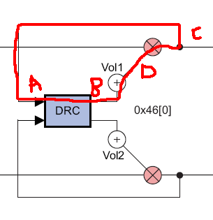
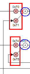
But now ,in TAS5713,there are two DRC,upper band DRC and lower band DRC,in one chip.

I have studied your DAP process in TAS5713 datasheet ,and try to understand how it works ,but something in it always confuse me ,and now I still don't know how to configure them to have a better performance compared to TAS5708 using MCU or GDE.

So, do you have something detailed which can tell me how two band DRC works,or can you tell me something which I can according to ?

 By the way ,in TAS5708's datasheet ,I know how DRC works.The structure can calculate the gain of audio data and multiply it to the input of DRC.

But in DAP process of TAS5713's datasheet, I just can't get the  meaning of input of DRC. It seems like that the input of DRC is output of all DAP ,and the gain of DRC seems not  multiply to the input of DRC. Here is the problem .Could you please tell me how it happens?

thank you !!!!

from zhuo yue

  • Hi, Zhuo Yue,

    I have asked my colleague to work with you on this. He is a little bit busy right now, so it might be next week before he gets back to you.

    -d2

  • hi Don Dapkus,

    Thank you for your response. It's none of business and I will wait until next week.

    zhuo yue 

  • While waiting for your answer, I’m still working hard to study the DRC structure in order to configure them for a better performance.

    First, Let’s discuss the following structure.

    The red line which has been highlighted seems to form a ring, which means that the output of DRC (point C) feeds back to the input of DRC (point A), where I can’t find a mark or math symbol such as Z-1 or something else. So, in my mind, my understanding is that the first audio data is processed by DRC over and over again until the next audio data come , which seems to be a wrong definition. Could you please give me an explanation for it?


    Next, my confusion is that how volume gain cooperate with DRC structure in TAS5713. In the picture above, point B is the real output of DRC and it pass through the volume gain module to point D. Here is a adder act as volume gain. So the audio data B add the volume gain equals to new audio data D? My understanding is that a multiplier is more appropriate here. Am I right?

    And the last question is that how to combine the processed audio data of upper band DRC and lower band DRC. My attention is the register 0x70 and 0x71 and 0x74 and 0x75. But when I configure it in GDE and read the I2C log file. I find that both 0x70 and 0x71 equal to 1.0, both 0x74 and 0x75 equals to 1.0 , which means that the processed data of Ch1 of upper band DRC add the processed data of Ch1 of lower band DRC. To be the same , the processed data of Ch2 of upper band DRC add the processed data of Ch2 of lower band DRC. Am I right? But it seems to be wrong again.


    I beg your time to answer me the three questions above, so I can configure the TAS5713 according to my requirement. Thank you more than once.

  • Can anyone help me ?

  • Sorry to touble you~

    But I still don't know how to balance two-band DRC and still waiting for your kind answers.

    zhuoyue