This thread has been locked.

If you have a related question, please click the "Ask a related question" button in the top right corner. The newly created question will be automatically linked to this question.

TPA3116 Board Issues

Other Parts Discussed in Thread: NE5534

Hello,

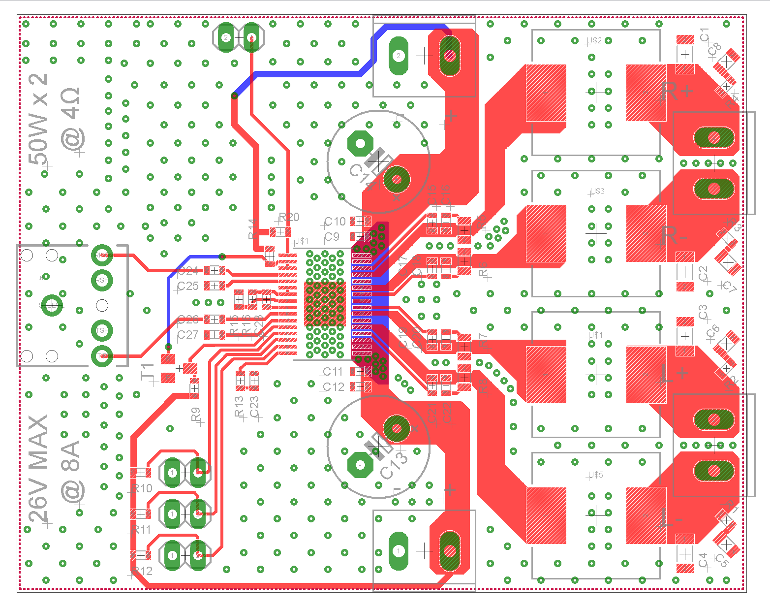
I have a new design that I have been trying to test. However, the TPA3116 is going into immediate fault when it is powered on. Here are the troubleshooting steps that I have performed so far:

  • Check short between all outputs and POSITIVE power input
  • Check short between all outputs and GND
  • Check for shorts between output pins
  • Check for shorts between POSITIVE power input and GND
  • Check for shorts between each and every pin on the IC.
    • Obviously SDZ and FAULT are tied together
    • PLIMIT and GVDD are also tied together
  • Use oscilloscope to watch the FAULT pin
    • The IC is not resetting itself. Once the chip is powered on, FAULTZ goes low (I'm reading 0.59 Volts on this pin) it goes into immediate fault and does not recover. I can watch the scope and you can see fault go high as the battery is plugged in, but immediately goes low and stays that way.
  • Use oscilloscope to watch for DC offset on the outputs
    • I'm not seeing any DC offset at all when the chip is powered on. It goes into fault far too quickly to get a reading here
  • Use multimeter to watch for over current condition
    • I don't think my multimeter would read this accurately anyway. Once the battery is plugged in it goes into immediate fault and the first current reading I get is the quiescent current (around 0.3mA MAX)

Here is my setup:

  • Test board
  • Battery Powered:  11.1V Lithium battery with 80A continuous discharge and 160A burst discharge.
  • 6 ohm speakers
  • 26dB Gain setting (100K and 20K gain resistors)
  • 1uF input caps
  • Single-ended input (can see how I do that in the schematic) using a 3.5mm headphone jack

Here are the images of the schematic and the board:

  • Hi, Billie
    Please provide the Fault and OUTx (Before filter) waveform when the fault occurs(High to Low) to me.
  • Billie,

    I had the same issue. This type of design uses differential input capacitors. One is tied to ground, the other is floating. If the input is left floating (not terminated) it causes a momentary differential input voltage on one or both channels since the capacitors are not charged equally. This causes the output to exceed the current limit, which in turn causes a fault. Try terminating your input with some sort of load. I ended up adding a 1k resistor to ground on the un-terminated cap. This seems to help a bit when testing with an un-terminated audio input.
  • Sorry for the delay. I accidentally fried the board that was showing this issue yesterday. However, I have started to assemble another board. Here are the results:

    I started assembling this board one component at a time. I put the chip on first, then put on all of the required pull-ups and gain resistors. Then I tested the voltage of the fault pin. I got a reading of 11.25 volts (the battery is 12.45 volts, but I'm assuming that the fault pin is causing the drop). This means that the chip should be working properly.

    Then I installed the inputs capacitors. Instead of installing the 1uF that I was originally using, I installed 4.7uF, whcih is closer to the 3.3uF suggested by the datasheet for the gain that I am using. As soon as I installed those, I could see with my multimeter that the fault pin was going high, then registering a fault. It's now stuck in this loop.

    Looking at my board, you can see that I am attempting to use this chip in single-ended mode. Can you see any design flaws that would cause my DC offset to be so high? I know the datasheet recommends ac coupling the inputs as close to the input as possible, but does my design really make that big of a difference?

    Also, there is a part of the datasheet that talks about single-ended mode. It says that you should AC couple the negative input to ground. Then it goes on to say that you should apply the input signal to one of the inputs, then AC ground the other inputs. Is it still referring to the negative inputs in this sentence, or is it saying to only apply a signal to one of the POSITIVE inputs, then AC ground the other positive?

    Any help at all is much appreciated.
  • So, you can't see this from the image of the board, but in the schematic you can see that I am using a 3.5mm input jack that has the switches internally. Those switches ground the positive input when a cable is not inserted. Also, I have been testing this design with various devices plugged in and playing music. I still see the same issue.
  • Here is some new information:

    After finding that installing the input caps caused the chip to trip the DC offset fault, I decided to try BTL mode. As suggested in the datasheet I tied the LINP and LINN to GND and then applied power to the chip. Much to my surprise, the FAULT pin was HIGH.

    Keep in mind that on this second board I still have not installed ANYTHING on the output yet. No caps, no inductors, nothing. The only components I have installed are as follows:

    - All 4 input caps (4.7uF)
    - Bypass Cap on the GVDD pin (1uF)
    - Pull-Up on Shutdown Pin (100K)
    - FAULT and Shutdown are shorted together
    - Gain setting resistors (100K Top and 20K bottom, 26dB Gain)
    - Pull-Up on Sync (4.7K with 47pF cap)

    No bypass or bulk caps have been installed on the power supply.

    Tomorrow I plan to breadboard a single-ended to differential converter (using some NE5534 op amps that I have) and then modifying the board so that the input caps are standing on end on the solder pad. The end that's up in the air will be tied to the output of the se-to-diff board. Let's see how that works out.

    In the meantime, if there are any suggestions to eliminate the DC offset that I'm seeing, I'd really appreciate it.
  • Hi, Billie 

              In order to make this device work normally, you need install Bootstrap capacitor (these 0.22uF capacitors on your board).

              BTW, I still think the board should work normally if these component value are the same as your schematic and there has no soldering issue.  

              If this is a DC detection fault, you can disable it with 1SPW mode (this is just a debug method for you).

  • Ok, today I put the chip in 1SPW mode (it was already there, but I confirmed it) and then I put the .22u bootstrap caps on and was still seeing the chip faulting every second or 2. I then pulled the 4.7uF input caps off and just as I suspected, the fault didn't occur again. I'm totally lost with this board. I tried jumping up to 10uF input caps (these were electrolytics instead of ceramics) and was still seeing a fault. The only thing I know to do to save these boards is to design a single-ended to differential converter adapter to deliver a differential signal.

    Still, I'd love to figure this out. Maybe I'll spin another batch of boards with better routing and input cap placement on the input lines and see how that works.
  • Billie,

    I noticed that you have Mute, Shutdown, and Fault all tied to VCC. This means that the PA will unmute at the same time as it is enabled. This will cause the PA to glitch and go into protection. I found that it is very important to unmute one or two seconds AFTER VCC is applied.

    Hope this helps.

    Mike