Hi Team,
My customer would like to evaluate TAS5719. For the DVD and PVDD, cusotmer would like to know the analog and digital power/ ground separation inside of chipset.
Could you provide your comment for this gnd layout?
Thanks,
SHH
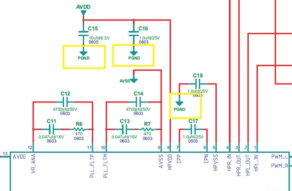
Hi Team,
My customer would like to evaluate TAS5719. For the DVD and PVDD, cusotmer would like to know the analog and digital power/ ground separation inside of chipset.
Could you provide your comment for this gnd layout?
Thanks,
SHH