This thread has been locked.

If you have a related question, please click the "Ask a related question" button in the top right corner. The newly created question will be automatically linked to this question.

TPA3144D2: The resistance of the voltage divider of GVDD for TPA3144D2

Part Number: TPA3144D2
Other Parts Discussed in Thread: TPA3140D2

Dear Sirs,

My customer asked us about the resistance of the voltage divider of GVDD for TPA3144D2.

The following description is on page 12 of the data sheet of TPA3144D2.

”The resistance of the voltage divider should be a minimum of 100 kΩ in order not
to overload the GVDD regulator of TPA3144D2.”

On the other hand, the following description is on page 17 of the data sheet.

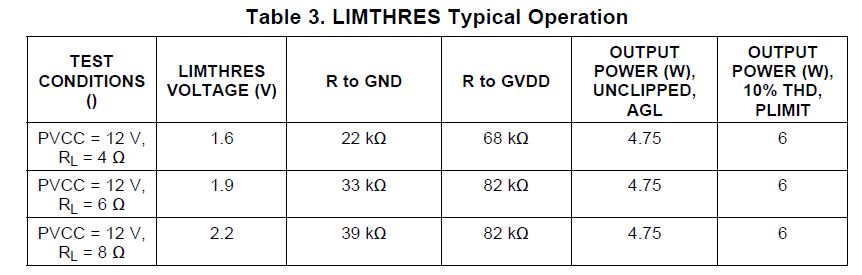
Under the condition of PVCC = 12 V and RL = 4 Ω
Voltage dividing resistance value is 90 kΩ and less than 100 kΩ.

Please tell me the correct value (description)?

Best  Regards,

Y.Hasebe

  • Hello Hasebe-san, SHawn can answer further questions for you, but Section 9.3.1 Gain Setting & section 9.3.7 LIMTHRES are illustrating two conceptual design views that may not coincide in all design use cases. What are the key elements of your design: AVCC/GVDD, gain, load type, etc...
    Also, please check out our newer TPA3137, which is a much more efficient inductor free, ultra low EMI device: www.ti.com/.../TPA3137D2 Thanks, Jeff
  • Hello Jeff-san,

    Thank you for your reply.

    The question is that the difference in the data sheet description and the split resistance value of TPA3140D2EVM is less than 100 kΩ.
    The key element of the design is Gain LIMIT setting.                                                                       (My customer is using TPA3144D2 but because I do not have EVM, I am substituting TPA3140D2EVM.)

    Regarding the division resistance value of EVM, it is a value for determining the voltage of LIMTHRES and it is recognized as convenience.
    Therefore, we actually recognize that it is recommended to design it according to the contents described in the data sheet on page 12 and Table 3 on page 17
    Is this correct?

    However, one condition in Table 3 on page 17 of TPA3144D2 data sheet does not satisfy 100 kΩ or more.
    I think that the reason for this is that TPA3144D2 has a small output relative to TPA3140D2.
    Is this correct?

    Best Regards, 

    Y.Hasebe

  • Hi Hasebe-san,

    In TPA3144D2 datasheet, a minimum of 100kohm load on GVDD is described. This number(100kohm) reserves some margin, so it's just a recommendation not a must. According to our designer, there isn't any problem for an as low as 50kohm load on GVDD. So the exampe on page17 in the datasheet is safe.

    About the load on GVDD, we need to take the following considerations:

    1. GVDD driving ability. It's mA level on TPA3144D2.  

    2. Shut-down current. In shut-down mode, GVDD is still working, then the current through the load on GVDD needs to be considered. Too low load on GVDD causes high current consumption.

    3. When the device starts up from shut-down mode, GVDD is also used to charge the Bootstrap capacitors. Need to make sure the current on through the load is not too large so that GVDD has enough ability of charging the Bootstrap capacitors.

    For TPA3144D2, there isn't problem for 50kohm load on GVDD. If you could use more than 100kohm load, it's even better.

    Best regards,

    Shawn Zheng

  • Hello Shawn-san,

    Thank you for your kindly reply.

    I understand your detailed comments.

    I will answer your comments  to my customer.

    Best Regards,

    Y.Hasebe