This thread has been locked.

If you have a related question, please click the "Ask a related question" button in the top right corner. The newly created question will be automatically linked to this question.

!CLIP always active

Other Parts Discussed in Thread: TAS5613, TAS5630Normal 0

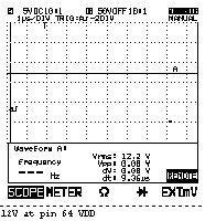
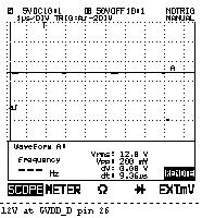
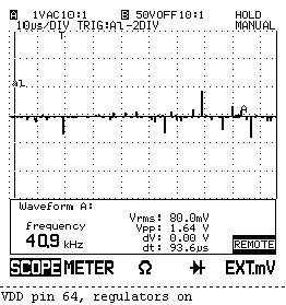
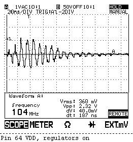
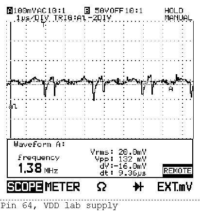
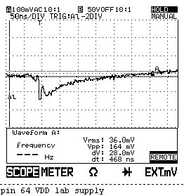
I am debugging a 5613-prototype card, not the TAS5613 evaluation card.  When power is on and reset is off, the amplifier is in a state where the CLIP signal is always on – even when there is no signal applied.

I am using components that are the same value or similar to the evaluation card which works in our application.  When applying a sine wave signal to the input, the output does not look clipped, but the sound heard from the speaker is very distorted.

 Any ideas on what the problem could be?  Or where to start looking for problems?

 Thanks,

Bruce


  • Bruce, can you compare the EVM to your circuit point by point (DC voltages, AC waveforms, etc)?  I think that could point to the answer.  Those are the data I would use to try to identify the problem.

    Also, please make sure your components are equivalent to those in the EVM.  For example, please make sure your LC filter inductors have the same saturation current as the EVM inductors (about 20A) and your filter caps have similar voltage and current ratings as the EVM caps.

    Best regards,

    Steve.

  • Ok, I will compare it to the EVM, and try your other suggestions.


    Thanks,

    Bruce

  • Normal 0

    I compared the output waveforms at the chip (OUT_D, BST_D) no load and the evaluation card is at 50% duty cycle with a 1.2us pulse width ~400KHz.  My prototype card output has a pulse width of 200ns, 8% duty cycle ~400KHz.


    The other pins on the chip seem to be similar between the two.  Except the CLIP is low on the prototype and the PSU_REF, VI_CM is at 1.20V on the prototype card and 1.70V on the evaluation card.


    I am using the toroid inductors and output capacitors removed from another evaluation card on the prototype card.


    Can you help point me in the right direction as far as what the problem could be?


    Thanks,

    Bruce

  • I changed some things:

    OC_ADJ from 30K to 22k.

    And moved the cap on VI_CM closer to the chip pin.


    Result, with no load  - VI_CM went up to 1.4V and the pulse width on OUT_D doubled from 200ns to 400ns.

    I am still in desperate need of help.  The clipping signal is mostly pulses now - which is an improvement, but far from what it should be. 

    TI technical support is down - due to bad weather.  Any help would be greatly appreciated.

    Thanks,

    Bruce

  • Bruce, I hope your weather is a lot better than ours.  I will try to help, but I think I need more information, which I hope you can post back to me.

    Changing Rocp from 30k to 22k increases the current limit, and in your case the output pulse width, and that suggests that something is drawing excess output current.  The fact that moving the VI_CM cap helped suggests issues in your PCB layout.  I always encourage our users to follow all the application notes in the data sheet SLES220B, especially the section called Printed Circuit Board Recommendation.  Also, it's best to make the layout very similar to the EVM layout - in fact, our users are welcome to copy it, and I encourage them to do so.

    That probably can't help you very quickly, so I would like to have a look at your schematic and layout.  I will need copies in PDF.  I will look for the cause of the problem.

    You may not want to post them on the forum.  In that case please send them to tempforum@list.ti.com.

    Regards,

    Steve.

  • Thanks for responding.  I'll email the data to you.  The information and application is confidential.

    Everything went back to 1.2V at VI_CM and 200ns at OUT_D.  I am still trying to figure out why it got better for a few minutes and then reverted back.


    Keep in mind that my test set up is open circuit load - nothing connected to the outputs.  No current flowing out of the outputs - except maybe the filter network at the output.  I am also not applying any audio signal to the 5630 inputs.  I am running the 5630 prototype without a heat sink, so that I can probe the pins.  The temperature of the chip is steady at 150F at the hottest point when running like this for testing purposes only.

    The eval. card (happens to be a 5613) is running without a heat sink also, and it is fine (no clipping with no-load and no-input).


    Sorry about your weather, it's cold here too - but not as much.  ....Wish I had the day off though...:-)

    Bruce

  • Bruce, TAS5630 typically won't run for very long without a heatsink - the package theta-JA is not high enough.  The device depends on heatsinking, with thermal grease to ensure a good thermal contact and with the heatsink grounded to shunt stray substrate currents.

    What happens if you add the heatsink?

    Regards,

    Steve.

  • Nothing.  It's the same with or without the heat sink.  Same goes for the eval. card - except the eval. card works better - the CLIP LED never flashes and the OUT_D is 50% duty cycle.  I don't need it to run very long for testing.... just a few seconds to check the CLIP signal.  I even tried grounding the thermal pad and that had no affect at all.

    -Bruce

  • Another piece of information:  I have an MCU monitoring and logging data on the card.

    I just checked the recorded status when I was getting 400ns pulses on OUT_D, 1.4V on IV_CM, and CLIP was mostly pulses.  It turns out that OTW1 was low.  So things were looking better when the chip issued an over temperature warning of 100C.

    And after it cooled off, it went back to 200ns on OUT_D and 1.2V on IV_CM.

    I am not sure if that is helpful…. It had been running 15 - 30 minutes while I was taking measurements when this happened.

    -Bruce

  • Bruce, it's possible there is damage to the IC somehow.  If you have time and feel it's critical enough, you might try this, unless you already have.

    Otherwise I will have to try to comment when I get your files.

    BTW, you mention only OUT_D.  Do the other outputs behave the same way?

    Regards,

    Steve.

  • I sent the files last night.  I'll re-send them now.

    The other outputs behave the same way.

    I doubt that the IC is damaged.


    -Bruce

  • I may have solved the problem.  I turned off the two switching regulators and substituted a lab supply for the 12V and other voltages and OUT_D looks clean and is at 50% duty cycle.  The switching regulators switch at 300KHz.

    The !CLIP signal is steady at 800mVDC.  I put a 3.3V 10K pull-up on !CLIP and it came up to 3.3V.

    I thought there was an internal pull-up on !CLIP.

    What do you think about:

    1. Why a 10K pull up is needed on !CLIP?

    2. Choosing a switching regulator that is more compatible with the 5630?


    Thanks,

    Bruce

  • Bruce, I still did not receive your files, because of a problem in the temporary address.  I believe that is fixed and you can resend the files, and this time I should receive them.

    But I will try to answer from what you have told me here.  Obviously, if the power supplies are not stable, performance cannot be predicted.  You are very welcome to copy the regulator circuits from the EVM, which were chosen for compatibility with TAS5630.

    /OTW1, /OTW2 and /SD have moderate internal pullup resistance, nominal 26k to VREG.  I will check about pullup on /CLIP.

    What is your resistance at FREQ_ADJ?  For 300kHz operation it must be 30k.

    Regards,

    Steve.

  • Hi Steve,

    Thanks for your help.  I will send the files again.

    It's the voltage regulators that are switching at 300KHz, the 5630 is switching at 400KHz (10K resistor).

    I know the regulators on my card are interfering with the operation of the 5630.  At this point I don't know if the regulator layout or circuit can be made any better than it is.  I noticed that the switching frequency of the regulators is pretty close to the switching frequency of the 5630.  And I noticed that on the 5613 evaluation card the voltage regulator is switching at 52KHz.  Could the switching frequency of the regulators on the card be the problem?   Is higher (1MHz) or lower (50KHz) better?

    -Bruce

  • Bruce, I received your schematic and layout.  There may be some issues there, but, before we go into that, can you take a look at all your power supplies, including your labe 12V supply and your switching regulators, at the TAS5630 pins?  Take scope shots and send them to me.

    Regards,

    Steve.

  • I cut the trace between the MCU input and the !CLIP output and the MCU input pin is floating at 800mV, the !CLIP output is zero Volts - Important: This is measured without a pull-up on !CLIP, it stays high with a pull-up.

    All other logic levels are at 3.20V (READY, !OTW1, !OTW2, !SD)

    Attached are some scope images:

    Zooming in:


    So it looks like there is +-1V of noise using the regulators and 100mV of noise with the lab supply.

    -Bruce

  • Bruce, where are you connecting your probe ground lead?  I hope at the chip itself.

    Also, can you check PVDD at the chip, too?

    Regards,

    Steve.

  • Steve,

    I replaced the 5630 chip and !CLIP is working now.  It is normally high and starts going low in pulses as the output peak reaches PVDD (30V for this card).  The output is also very clean after disabling the switching regulators.  So I am looking at replacing that part of the circuit with a switching regulator that is more compatible with the 5630.


    Other than the switching regulator issue, I tried to stick as close to the evaluation card layout as possible.  Do you see any room for improvement on the output side of the 5630, or anywhere else around it?


    Thanks,

    Bruce

  • Bruce, I am concerned about the layout around TAS5630, because it is rather different from the EVM.  The data sheet points out several things that are important to performance in the section called Printed Circuit Board Recommendation, and the EVM should serve as a guide to layout.  I do not see these implemented in your board.

    - Your bulk decoupling cap placement is OK, but the 1uF decoupling caps should be on the top layer immediately beside the PVDD and GND_X pins.  As it is, they must be connected through vias, which add inductance, and there is no strong ground connection to the GND_X pins.  You may see high overshoot and ringing between GND_X pins and PVDD pins and outputs as a result.

         (This is why I wanted to see PVDD measurements, to see if the decoupling is good enough or not.)

    - You're using 50V caps on PVDD, which may be OK if PVDD is a maximum of about 30V and the caps are made of X5R or better material.  But your top silkscreen says 25 to 40 V, and I would recommend higher voltage caps for PVDD of 40V.  The reasons for the choices of materials and voltages are explained in the attached presentation on circuit design for class-D.

    - Your ground plane is broken in many areas, especially under the device.  There is no clear strong path from the device to the PVDD connector or to the bulk decoupling caps or the output filter caps.

    If you are satisfied with the performance of your board as it is, then it will not be necessary to improve it.  But please be aware of the potential for issues in audio performance and EMC.

    Regards,

    Steve.

    Crct-dsn-home-ent-audio+EMC-100818.pdf
  • Thanks for your input, I'll take a look at the 1uF caps, and ground plane on the next spin of the card. 

    And yes - the supply is 30V.  But your point is well taken - when I did the silkscreen I was thinking about the regulator (could go to 42V) and forgot about the capacitors.

    Thanks for all your other help on this thread too.

    -Bruce