A related question is a question created from another question. When the related question is created, it will be automatically linked to the original question.
If you have a related question, please click the "Ask a related question" button in the top right corner. The newly created question will be automatically linked to this question.
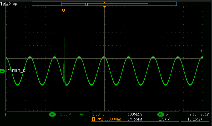
PCM5121: Asking for the PCM5121 schematic and layout review
I suspect that the glitch is due to corruption of the I2S signal. What speed is it operating at? Is it geographically laid out near hi-power or switching signals?
Hi Paul,
In the PCM5121 spec sheet, Timing Requirements of SCK is defined in page 11, but other I2S signals timing are not defined.(BCK, DATA, LRCK)
Do you have any solution and could you get signal timing spec and any comments for this issue ?
Currently, customer is using I2S as 3 wire mode (BCK, DATA, LRCK, not use SCK) by FW setting.