A related question is a question created from another question. When the related question is created, it will be automatically linked to the original question.
If you have a related question, please click the "Ask a related question" button in the top right corner. The newly created question will be automatically linked to this question.
Part Number: PCM1865 Other Parts Discussed in Thread: OPA2350
Hi, Zak,
If working in 4ch with I2S mode, it must use the SDO2 pin for the other 2ch data? If in TDM mode, there is just one SDO needed ,but must run BCK at a higer frequency , 256XLRCK, right?
Further more, if comparing with low noise opa2350 , could the PGA inside the ADC outperform the former in the noise figure? I was considering the gain distribution between the front OPA and the inside PGA and could you please give some advice?
There is no way to bypass the PGA inside the PCM186x, but based on the specs we can do a rough calculation of its noise. With 0dB gain the SNR is 110dB, and with a full scale range of 4.2Vrms this means the input referred noise would be ~13.3uVrms. With 32dB gain the SNR is 90dB, or ~132.8uVrms. You can assume that the PGA noise is dominant at this point and just divide by the gain to approximate the PGA noise, or actually go through the additive noise calculation and you will find that the PGA noise is approximately 3.32uVrms and the ADC ~12.88uVrms under datasheet test conditions.
Assuming a 24kHz bandwidth of integration this would translate to ~21.4nV/rtHz. Since you can't bypass the PGA it will always add some noise but at high gains you may see somewhat better SNR using the OPA2350 depending on how you configure it and how much noise your circuit contributes outside of the intrinsic amplifier noise.
Further testing show that there have a a little higher leakage of the fs/4 component in the output , regardless of the fs either 96k or 192k . The leakage is about 5-10db above the output noise floor and will disappear if running at fs 48k. The ADC is powered by the the LDO +3.3v, and the system is powered by a bulk mode DC-DC converter +5v , which is synchronized to 384k ,twice of the max fs 192k. Where might the fs/4 signal come from? could you please give some advice ?
We are running the adc in a sampling detector with the full signal bandwidth of fs/2. When no signal input, the adc should output the flat backgroud noise floor after the FFT. There have some peak signal at the fs/4 when fs=96k or 192k. The level will be 5-10db higher than the floor. But when fs=48k, the backgroud is much clean than above. The peak signal seem some kind of leakage inside the adc, and outside the 20khz audio bandwidth. Any possible reason, could you please give me some advice ?
The PGA have been set to the maximum 32db without signal input. The 3.3v VDD is from a dc-dc converter which was synchronized to 384KHz. Do you think the fs/4 component is coming from the intermodulation interference of the spike from the dc-dc converter? But why is the fs/4?
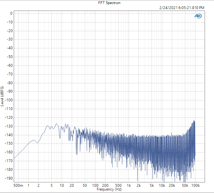
Please refer to the attahced. This is the FFT result of the ADC data. The full span is Fs= 192k and the 2 spike near the center is the +-Fs/4 leakage signal, with the level +13db higher than the noise floor. If change Fs to 96k, the spike is still the same position, but just 7db higher than the noise floor.
I am running the adc in 4CH mode and left the other 2CH input float. There have not such Fs/4 clock on my board and the Lowest clock is the LRCK ,192K, and the BCK is 6.144Mhz. So I can not image where is the leakage coming from. Inside or outside the chip?
Thank you for sharing more system details. I'm not sure exactly where this tone is coming from. I would recommend trying a couple things:
1) If you can, change the switching frequency of your DC/DC converter, or drive the PCM186x from an LDO or a battery to see if the behavior of the tone changes.
2) Measure with lower PGA gain to determine if this is arising from the front end or in the modulator. If it changes with PGA gain this may be an idle tone, and I will try to verify this on my end.
I apologize for the delay as I was out of office for the past week. I am going to see if I can recreate this behavior on our EVM, but due to conditions in Dallas from the recent snow storm I will not be able to get into the lab until next week. Please let us know if you have found any resolution on your end!
No progress now. We doubt the leackage must have some relationship with the Fs. There have 6 kind of fixed clock source in my broad, 24Mhz , 25Mhz, 98.304Mhz, 6.144Mhz, 96Khz and 384Khz. Considering the leackage were around +10db above the noise floor and so weak, which clock could be the main reason?
I don't think I was able to reproduce quite what you are seeing but am attaching some data for reference. I measured an FFT on the device running at 192kHz with a TDM256 interface. The noise does start to increase above FS/4 in this case, but I'm not sure if this is quite the same as what you are seeing. If it is, then this is a characteristic of the device filters at these higher sample rates.
It seems the leakage is coming from the ground noise coupling from the MCU. The strong common mode noise might leak into the L and R channel preamplifier before the ADC through the power rail. I am using the single end input mode for ADC and how about the diffirential mode for the common noise suppression?
I am glad you were able to find the noise source! If the noise is leaking in through the supply of the preamp then the differential input will help reject any common-mode interference assuming the noise is passed through as common-mode. I think it is definitely worth trying. If this is a ground bounce problem around the PCM186x though then the issue could be that the reference voltage is being modulated and differential inputs won't help with that. It is still a worthwhile experiment though to see if you can adjust the input circuit or if more care is needed in the ground plane management.