A related question is a question created from another question. When the related question is created, it will be automatically linked to the original question.
If you have a related question, please click the "Ask a related question" button in the top right corner. The newly created question will be automatically linked to this question.
Hi Will,
I think you can use the BTL mode data in the same case(PVDD, Load, input frequency). it would be very similar for PBTL mode. In PBTL mode, the output current is divides into two halves, it actually decrease the current in each channel and then improve the thermal performance. But it doesn't improve the linearity range much.
In PBTL mode, the PBTL pin needs to be driven to High level. And the output OUTA after LC filter and OUTB after LC fitler are combined. The same is OUTC and OUTD. Please find more info in our TAS5717 EVM user's guide for PBTL mode config: www.ti.com/.../slos655a.pdf
Best regards,
Shawn Zheng
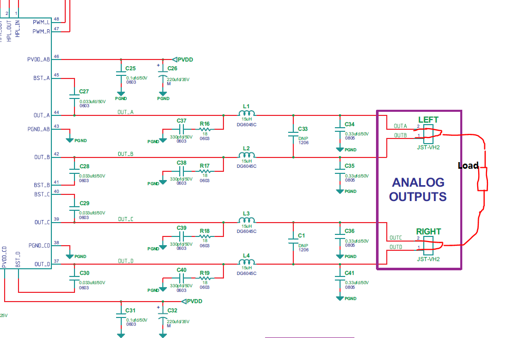
I appologize for the confusion. It is a typo in the document, please ingore that description. The following picture shows the PBTL connection. Short OUT_A and OUT_B after the LC filter, short OUT_C and OUT_D after LC filter. Connect the load between them. Make sure the register 0x25 is set to 0x01 10 32 45 for PBTL mode.