


Part Number: PCM3060
Hello everybody,
I fail to power up the PCM3060. I followed the power up sequence described in the manual (p. 16-17). Tried and validated many things and now I got no clue where to seek the root of the issue.
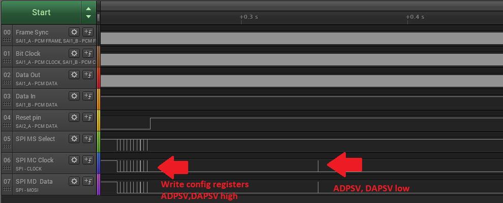
My power up sequence is:
- Reset pin low
- Write the configure registers over SPI (~0,5MHz)
- Reset pin high
- ADC-,DAC power save on (over SPI)
- Wait for 100ms
- ADC-,DAC power save off (over SPI)
- Nothing happens: No data from ADC. DAC output fixed to VCOM. No life reaction from the device
Additional infos:
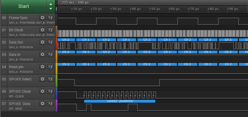
- Both DAC and ADC should work as slave using the BCLK2, LRCK2. The pins BCLK1, LRCK1 and SCK1 are floating.
- LRCK=48kHz, BCLK=3072kHz, SCK=12288kHz
- MODE pin at VDD for SPI mode.
- VDD is ~ 3.65V
- VCC is ~ 4.8V
- All pins including BCLK2, LRCK2, SCK2, SPI modes are validated using logic analyzer /osci /multimeter. All are getting correct signals / frequencies.
- SPI values validated: All being sent correctly.
Signal analysis of the power up sequence captured directly from the device pins:
Zoomed to the first SPI message: ("Data Out" is the Data in for the DAC, "Data in" is the output from the ADC)
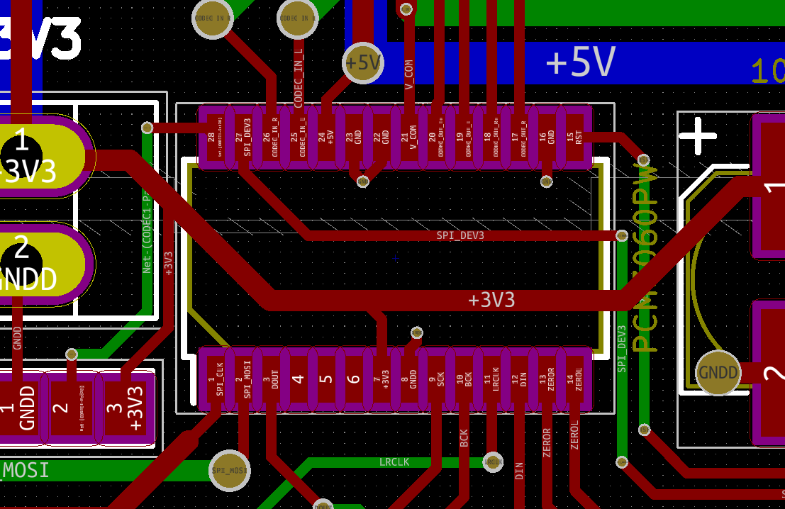
PCB:
C-Code of the configurations and power up sequence:
void init_pcm3060(void){
printf("Initializing PCM3060\n");
int i=0;
uint16_t reg[10];
uint16_t reg_release=0;
//Regs
reg[0]=
64<<8 //Register id
|0<<7 //MRST: Mode control reset (0=Set to default)
|0<<6 //SRST: System reset (0= Resync.)
|1<<5 //ADPSV: ADC Power save control (1= power save)
|1<<4 //DAPSV: DAC Power save control (1= power save)
|0; //S/E: Singled ended or differential select (0=diff)
reg[1]=
65<<8 //Register id
|255; //DAC Attenuation level left (255=No attenuation)
reg[2]=
66<<8 //Register id
|255; //DAC Attenuation level right (255=No attenuation)
reg[3]=
67<<8 //Register id
|0<<7 //CSEL2: Clock select DAC (0= SCK2, BCK2, LRCK2 enabled)
|0b000<<4 //M/S: Master select DAC (0b000=Slave mode)
|0b01;//FMT2: Audio interface format DAC (0b01=24 bit LJ)
reg[4]=
68<<8 //Register id
|0<<6 //OVER: Oversampling rate control DAC (0=x32 Oversampling)
|0<<2 //DREV2: Output phase select (0=Non-inverted)
|0<<1 //MUT22: Soft mute control left (0=No mute)
|0; //MUT21: Soft mute control right (0=No mute)
reg[5]=
69<<8 //Register id
|0 //FLT: Digital filter rolloff control DAC (0=Sharp roloff)
|0b01<<5 //DMF: Sampling freq selection for De-Emphasis DAC (0b01=48kHz)
|0<<4 //DMC: De-Emphasis control DAC ( 0=Disabled)
|0<<1 //ZREV: Zero detect polarity (0=High)
|0; //AZRO: Zero flag function select
reg[6]=
70<<8 //Register id
|215; //ADC Attenuation level left (215==0dB)
reg[7]=
71<<8 //Register id
|215; //ADC Attenuation level right (215==0dB)
reg[8]=
72<<8 //Register id
|1<<7 //CSEL1: Clock select ADC (0=SCK1, BCK1)
|0b000<<4 //M/S: Master select ADC (0b000=Slave)
|0b01;//FMT2: Audio interface format ADC (01=24 bit LJ)
reg[9]=
73<<8 //Register id
|1<<4 //ZCDD: Zero cross detection disable (1=Disabled)
|0<<3 //BYP: HPF Bypass controll ADC (0=HPF enabled)
|0<<2 //DREV1: Input phase select ADC (0=Non-inverted)
|0<<1 //MUT12: Soft mute control ADC left (0=No mute)
|0; //MUT11: Soft mute control ADC right (0=No mute)
//Register for releasing the ADC/DAC power save mode
reg_release=
64<<8 //Register id
|0<<7 //MRST: Mode control reset (0=Set to default)
|0<<6 //SRST: System reset (0= Resync.)
|0<<5 //ADPSV: ADC Power save control (0=normal mode)
|0<<4 //DAPSV: DAC Power save control (0=normal mode)
|0; //S/E: Singled ended or differential select (0=diff)
//Startup and init sequence
HAL_GPIO_WritePin(GPIOG,GPIO_PIN_0,0); //Pull RST pin to low
HAL_Delay(100); //Wait for power-up
HAL_GPIO_WritePin(GPIOG,GPIO_PIN_1,1); //MS high: SPI Unselect device
HAL_Delay(10); //Wait
//Write configuration registers
for(i=0;i<sizeof(reg)/2;i++){
HAL_GPIO_WritePin(GPIOG,GPIO_PIN_1,0); //MS low: SPI Select device
HAL_SPI_Transmit(&hspi3,(uint8_t *)®[i],1,1000); //Send config register
HAL_GPIO_WritePin(GPIOG,GPIO_PIN_1,1);//MS high: SPI Unselect device
HAL_Delay(1); //Wait
}
//Starting up
HAL_GPIO_WritePin(GPIOG,GPIO_PIN_0,1); //Push RST pin to high
HAL_Delay(100); //Wait to release power save mode (100ms)
HAL_SPI_Transmit(&hspi3,(uint8_t *)®_release,1,1000); //Exit power save mode via SPI command
}
What am I missing? What else can I try? Is the device may be broken?

