This thread has been locked.

If you have a related question, please click the "Ask a related question" button in the top right corner. The newly created question will be automatically linked to this question.

LMK04208EVM: 76.8 MHz VCXO recommendation

Part Number: LMK04208EVM
Other Parts Discussed in Thread: LMK04208

HI,

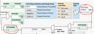
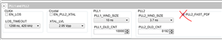
We would like to replace the VCXO on this board with 76.8MHz. Please provide TI recommendation as to the right part # for this. We currently have 122.88 VCXO on board.   

Thanks,

Syahriza Andiko

Intel Corp.

  • Hello Syahriza,

    The footprint on the LMK04208EVM should support both 5x7mm VCXO and 9x14mm VCXO. For 5x7mm, consider something like the 356P/L from CTS. For 9x14mm, consider the Crystek CVHD-950-76.800. If the best performance is required, I strongly recommend the Crystek VCXO, as nearly all other VCXOs on the market are lower performance (around 500fs typical).

    Regards,

    Derek Payne

  • Thanks.

    If we want to replace the VCXO with Crystex CHVD-950, is there any HW rework needed on the LMK04208
    EVM board to accommodate this VCXO?  

  • The U2 footprint is placed overtop of the U8 footprint, with compatible footprints. Two changes would need to be made:

    • The CVHD-950-76.800 only offers LVCMOS, so the unused differential pin should be removed. C38 should be moved to populate C40 instead, for single-ended VCXO input configuration.
    • LVCMOS signal swing is larger than the acceptable OSCin input range for the LMK04208; in that case, I recommend converting R17/C12/R12 to a 6dB pad (R17=151Ω, C12=37.3Ω, R12=151Ω) to attenuate the single-ended LVCMOS signal level to within acceptable limits.

    Regards,

    Derek Payne

  • What is the expected power level of OSCin_1_N?

    Replaced the VCXO with Cystexk CVHD -950-76.8M, and configured the board with 76.8MHz VCXO and 38.4 MHz CLKin1 but the LD LED is off. Not sure what's wrong, any suggestions? 

  • There's two critical requirements for OSCin or CLKin single-ended:

    • Slew rate > 0.15V/ns (ideally > 0.5V/ns)
    • Signal swing > 200mVpp (250mVpp CLKin)

    Given that the CVHD-950 76.8M is a CMOS oscillator, the slew rate requirement should be satisfied (even at reduced amplitude). And a 6dB pad would not reduce the CMOS amplitude below 200mVpp. I suspect the VCXO signal quality is not the issue. On the other hand, does the 38.4MHz signal satisfy these requirements for CLKin? Especially if 38.4MHz is provided with signal generator sine wave, the slew rate may be too low; sine wave slew rate is SR = 2π*f*Vpk, which works out to around +6dBm into 50Ω to meet the minimum slew rate requirement. If the 38.4MHz is a square wave or some other standard like LVDS, this concern probably doesn't apply.

    Next, have you ensured that the loop filter for PLL1 is still valid with a 76.8MHz VCXO? We offer PLLatinum Sim as a free tool that can help compute the loop filter values or check loop stability and phase noise performance.

    Assuming none of that is the problem, my usual next step is to switch the I/Os to show the PLL1 R and N signals, and inspect with an oscilloscope. The controls for switching the I/O signals are LD_MUX and HOLDOVER_MUX located in the "User Controls" page under the "Input Output" group. Inspecting the PLL phase detector inputs could identify issues with signal not being received:

    • No R signal - maybe CLKin_Select_MODE is not selecting the correct input?
    • Erratic or unstable R signal - potential signal integrity problem
    • No N signal - check PD_OSCin=0, confirm VCXO is powered
    • Erratic or unstable N signal - potential signal integrity problem
    • Incorrect but stable frequency of N - check charge pump polarity is correct, check charge pump is active and not tri-stated, ensure loop filter is stable, ensure CPout1 voltage = VTUNE voltage for the VCXO

    Regards,

    Derek Payne

  • There is no C40. Is this a typo? 

    We would like to revert it back to the original configuration (122.88 VCXO). What is the original value for R17/C12/R12? 

  • My bad, just ignore the above statement. 

  • Hi Derek,

    More question:

    In this eval board, from where can we measure these N and R signal?

    CPout1 voltage --> should be measured at VTUNE_TP???


  • Hi Syahriza, sorry for the delay:

    The CPout1 voltage can be measured at VTUNE1_TP, or at pin 34 (if you're feeling brave :)

    The N and the R signals will be exposed on the Status_LD pin and the Status_HOLDOVER pins in the scheme I suggested above. These are exposed at LD_TP and Holdover_TP respectively.

    In case you are still unsure about the original values, they are documented on page 18 of the LMK04208EVM User's Guide.

    Regards,

    Derek Payne

  • Thanks Derek.

    Is the loop BW of PLL1 or 2 function of VCXO freq?  Would like to make sure whether 20 Hz loop BW of PLL1 is fixed or not.  

  • Hi Derek,

    With 122.88 VCXO, is the value below making any sense (LD LED is ON)? 

    Vtune1_TP= 1.5V

    LD_TP= 3 V

    Holdover_TP= 0V 

    I'm kind of confused with "N and R signals" . Are these control signals or the actual clock signal?  

  • Syahriza,

    If the VCXO gain scales with the frequency (i.e. if the gain in PPM/V is the same for both VCXO frequencies), then all else being equal the loop bandwidth should remain unchanged.

    I don't think I explained this clearly: you can actually set the Status_LD and the Holdover_LD pins to display signals other than the lock detect status or the holdover status. Some of the signals you can route out of the device are buffered copies of the signals at the PLL1 R/N divider outputs, or in other words the inputs to the PLL phase detector. Routing out the divider outputs, i.e. the phase detector inputs, can help to diagnose some of the lock issues you might be seeing. I included an image below to clarify how to configure the Status_LD and the Holdover_LD pins:

    Regards,

    Derek Payne

  • Hi Derek,

    We replaced the VCXO with Crystek CVHD-950-76.800 and did the recommended rework. Also we replaced the below external loop filter components for PLL1. 

    1. C1_VCXO  -> 18 nF
    2. C2_VCXO -> 820 nF
    3. R2_VCXO --> 33kOhm

    With Freq Ref 38.4 MHz on CLKin1, we are not observing LD. (also there is no N signal observed (LD_MUX = PLL1 N)) 

  • Syahriza,

    It seems like the VCXO signal is not getting to OSCin, or else the OSCin buffer is routed in some strange way that's preventing the N-divider from toggling. Can you save your TICS Pro profile and upload it so I can review?

    Regards,

    Derek Payne

  • Found out that the VCXO was broken. Replaced the broken VCXO and now we could observe both N and R signals, but there is still no LD light. Btw, how can we upload files into this ticket? . 

  • Found out that the VCXO was broken. Replaced the broken VCXO and now we could observe both N and R signals, but there is still no LD light. Btw, how can we upload files into this ticket? . 

    38p4MHz_RefWith_VCXO_76.8_R_N.tcs

  • Here are the changes implemented:

    1. Replaced 122.88MHz VCX0 with  Crystek CVHD-950-76.800

    2. Replaced the following:

    1. C1_VCXO à 18 nF
    2. C2_VCXO à 820 nF
    3. R2_VCXO à 33kOhm

    3. C38 moved to populate C40

    4/ converted R17/C12/R12 to a 6dB pad à (R17=151Ω, C12=37.3Ω, R12=151Ω)

    After all the changes above, there is no LD signal observed ( Ref freq: 38.4MHz). Please take a look the observed N and R signals, and config file  in the previous comments.

    So not sure what the issue here. any comments? .  

  • Syahriza,

    With this configuration, are you seeing the VTUNE voltage at the VCXO pin close to 1.65V? It may be that the PLL is locked, but the lock detect window is set too tight. If you see a VTUNE voltage close to 1.65V, you could try setting the PLL1 window a little more relaxed at 40ns:

    If the VTUNE is still off in the weeds, next step can you try putting the charge pump output current to 1.6mA for debug? I see you have 0.1mA set, and I'm wondering if there's some VCXO input impedance or leakage issues that are impacting the current... 0.1mA is not that much current, so it sometimes isn't enough drive strength. Another possibility is the reduced 10Hz loop bandwidth isn't tracking some other noise source out e.g. 60Hz line noise from some system supply. I checked PLLatinum Sim and PLL1 should still be stable with the higher charge pump current.

    Regards,

    Derek Payne

  • Thanks Derek.

    Vtune is about 1.8 Volt. It is a little bit higher than what expected.

     Changed PLL1 window to 40 ns, also changed charge pump current to 1.6mA. There is no change in Vtune or LD 

    The other issue we are seeing is the  CLock4 out is not accurate, With the current setting (attached)38p4MHz_RefWith_VCXO_76.8_0526.tcs the output of ClockOut4 should be at 76.8MHz,what being measured is at 105.98 MHz    

  • Hi Syahriza,

    Apologies for the delay, E2E decided to hide my "reply" buttons...

    I see that the VCO is configured for 1843.2MHz, but you are using internal VCO. The VCO frequency range on LMK04208 is 2750MHz to 3072MHz. Did you perhaps mean to set the N-prescaler to 3, and the clock output dividers 50% higher?

    Also, in the user controls, I see you have PLL2_FAST_PDF=1. You should set this to 0 for a phase detector frequency <= 100MHz.

    Regards,

    Derek Payne