This thread has been locked.

If you have a related question, please click the "Ask a related question" button in the top right corner. The newly created question will be automatically linked to this question.

CDCI6214: Clarification on LDVS output settings

Part Number: CDCI6214
Other Parts Discussed in Thread: AM5716

Hi,

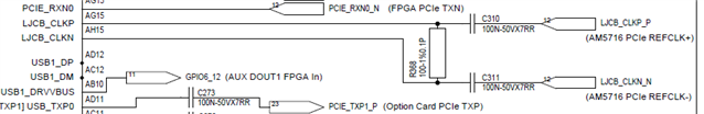
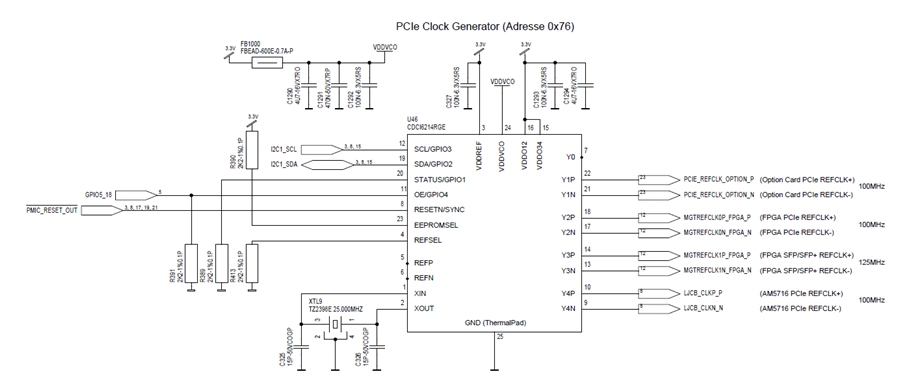
We have problems with some CDCI6214 in our products. On some devices output VOD is far less than the value from the datasheet. We use LVDS output. VDDIO12 and VDDIO34 is 3.3V.

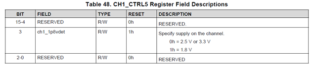
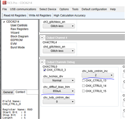
Prior to be more specific to the problem I want to have a clarification on the chX_1p8vdet setting. Some time ago I asked E2E if there is a risk of device damage when selecting EEPROM page 1 (with chX_1p8vdet set to 1) while having VDDIO12 and VDDIO34 at 3.3V. The answer was:


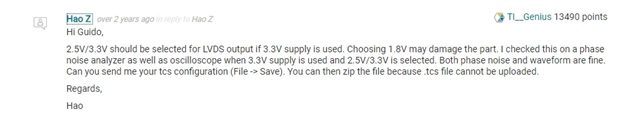
On an other E2E thread I can see that:
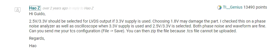
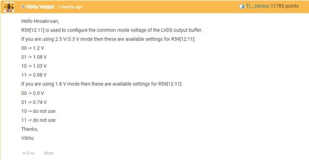
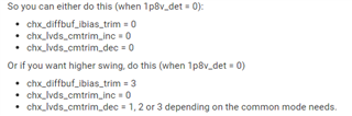


Or that:


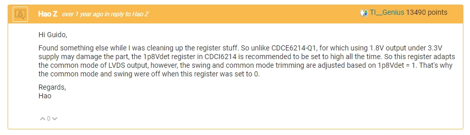
Can someone from TI please clarify the situation and tell me what exactly the chX_1p8vdet setting does. If there is a potential risk of a device damage it would be very helpful if this topic is described in more detail in the datasheet.

Thanks and best regards,

Patrick

  • Hi Patrick,

    Please refer to the datasheet statements.

    Possible reason for the lower VOD: 1p8v_det bit is set to 0, and common mode is set to too high. High common mode and high bias current will cause some trouble.

    So you can either do this (when 1p8v_det = 0):

    • chx_diffbuf_ibias_trim = 0
    • chx_lvds_cmtrim_inc = 0
    • chx_lvds_cmtrim_dec = 0

    Or if you want higher swing, do this (when 1p8v_det = 0)

    • chx_diffbuf_ibias_trim = 3
    • chx_lvds_cmtrim_inc = 0
    • chx_lvds_cmtrim_dec = 1, 2 or 3 depending on the common mode needs.

    The cmtrim_inc register increments the common mode. The cmtrim_dec register decrements the common mode.

    When 1p8v_det = 1 this problem should never happen.

    Regards,
    Hao

  • Hi Hao,

    Thanks for your advice.

    Our LVDS signals are AC coupled and terminated as needed. So that should not be the problem.

    In the datasheet I can read the following:


    So as VDDIO12 and VDDIO34 is 3.3V in our case, why should I set ch1_1p8vdet to 1h (1.8V)?

    You wrote in one thread that choosing 1.8V may damage the part:

    Maybe you can clarify the "Damage" statement for chx_1p8vdet setting while using 3.3V on VDDIO12 and VDDIO34.

    In the datasheet I can also read that when DC coupled output common mode voltage VCM is 1.2V (@3.3V) if chx_lvds_cmtrim_inc=2. From an other thread I read:


    So here common mode voltage is 1.2V when the chx_lvds_cmtrim_inc value is 0. But maybe just chx_lvds_cmtrim_inc and chx_lvds_cmtrim_dec was twisted. That is very confusing. Default value for both chx_lvds_cmtrim_inc and chx_lvds_cmtrim_dec is 0. Any feedback on this is also highly appreciated.
    Maybe the datasheet needs a complete rework on this topic. Maybe the correct values for VCM should be in the datasheet as well.

    To our specific problem:
    VOD is on some of our products with CDCI6214 too low. When testing maybe 1/3 of our products are out of tolerance. While testing the setting is always the same (chx_lvds_cmtrim_inc=2, chx_lvds_cmtrim_dec=0, chx_diffbuf_ibias_trim=3).
    chx_lvds_cmtrim_inc is set to 2 because of the datasheet telling VCM is 1.2V when setting chx_lvds_cmtrim_inc=2.
    Now we are unshure whether the devices (CDCI6214) are already damaged or the setting is somehow wrong.

    This topic is pretty urgent as "out of tolerance" product heap is getting bigger and bigger.

    Regards,

    Patrick 


  • Hi Patrick,

    Yes you should set the 1p8vdet bit to 0. But just follow my advice and set the ibias_trim to 0 and see if solves the problem.

    Regards,

    Hao

  • Hi Hao,

    I now had the possibility to analyse the problem. In one case I can see that the aplitude is fading from about 350mV to about 120mV in around 12s after enable of the outputs. It does not matter what I set in chx_lvds_cmtrim_inc or chx_lvds_cmtrim_dec.
    It would really help having a clear statement on the supply setting and if this setting can kill the device outputs or not.

    Regards,
    Patrick

  • Hi Patrick,

    Let me get back to you on this next Monday. Meanwhile, can you upload the configuration file you are using that produces this low amplitude issue?

    Regards,
    Hao

  • Hi Hao,

    Attached are the register settings of the CDCI6214. Also attached is the schematic of the CDCI6214 and the schematic of the AM5716 part where we use one of the clocks.


    R70	0x00460000
    R69	0x00450000
    R68	0x00440000
    R67	0x00430020
    R66	0x00420200
    R65	0x00410F34
    R64	0x0040000D
    R63	0x003F4210
    R62	0x003E4218
    R61	0x003D1500
    R60	0x003C0018
    R59	0x003B0069
    R58	0x003A0000
    R57	0x00398851
    R56	0x00380005
    R55	0x00370005
    R54	0x00360000
    R53	0x00358000
    R52	0x00340000
    R51	0x00338861
    R50	0x00320005
    R49	0x00310004
    R48	0x00300000
    R47	0x002F8000
    R46	0x002E0000
    R45	0x002D0851
    R44	0x002C0005
    R43	0x002B0005
    R42	0x002A0000
    R41	0x00298000
    R40	0x00280000
    R39	0x00270851
    R38	0x00260005
    R37	0x00250005
    R36	0x00240000
    R35	0x00238000
    R34	0x00220050
    R33	0x00210007
    R32	0x00200000
    R31	0x001F1E72
    R30	0x001E5145
    R29	0x001D400A
    R28	0x001C0000
    R27	0x001B0000
    R26	0x001A001C
    R25	0x00192406
    R24	0x00180000
    R23	0x00170000
    R22	0x00160000
    R21	0x00150000
    R20	0x00140001
    R19	0x00130000
    R18	0x0012FFFF
    R17	0x001126C4
    R16	0x0010921F
    R15	0x000FA037
    R14	0x000E0000
    R13	0x000D0000
    R12	0x000C0000
    R11	0x000B0000
    R10	0x000A0000
    R9	0x00090000
    R8	0x00080001
    R7	0x00070C0D
    R6	0x000619CA
    R5	0x00050000
    R4	0x00040055
    R3	0x00030801
    R2	0x00020053
    R1	0x00016820
    R0	0x00000010
    

    Further analysis show that when I measure the clock at C310 on the CDCI6214 side with an oscilloscope I can see that the clock is slowly fading away from normal level (approx. 330mVpp) to around 100mVpp. If I measure the clock at C310 at the AM5716 side the clock is stable at approx. 330mVpp. AM5716 is not running because it is held in Boundary scan mode.

    Regards,
    Patrick

  • Hi Patrick,

    You can find the explanation attached: CDCI6214_debug_general.pdf

    In Ticpsro, change these settings:

    To below:

    However, I don't know why clock swing is different on two sides of the capacitor (this is theoretically impossible). You can directly measure the clock on the two pads of the capacitor and go from there.

    Regards,
    Hao

  • Hi Hao,

    Thanks for the information.
    The strange thing is that if I measure on both sides of the capacitor with two probes the amplitude is ok as well (also with the settings I already have).
    That is why I want to be shure that the device will not get damaged while having "chx_1p8vdet" not set according to the applied voltage on VDDO12 and/or VDDO34. A clear statement about this topic is urgently needed.

    Regards,

    Patrick

  • Hi Patrick,

    I just received the confirmation from designer. When bit chx_1p8vdet is set to 1, the common mode voltage will be reduced to a very low value. If that's acceptable, then there's no issue. Setting it to 1 with VDDO = 3.3V won't damage the device.

    Regards,
    Hao

  • Hi Hao,

    That is good news. Thanks for the clear statement. So my first question is answered and I will close the thread although we still have this strange measurement effect.

    Regards,
    Patrick