This thread has been locked.

If you have a related question, please click the "Ask a related question" button in the top right corner. The newly created question will be automatically linked to this question.

LMK04828: Usage of the LMK device to generate required clocks and conditions if any

Part Number: LMK04828
Other Parts Discussed in Thread: LMK04832

Hi, 

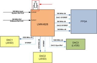
In our design, we are having clock requirements as per the below block diagram, currently planning to use the LMK04828 device for generating the clocks

We have the following queries on the same

  1. Is it possible to generate all the clock frequencies (as per the diagram) using the LMK device? What are your suggestions if any? Are there any conditions?
  2. In our design, we are providing 2 clock inputs, CLKin0 from a system clock source and CLKin1 from an onboard clock source, so these are the only clock sources available. In the LMK04828 datasheet, there is a "Simplified Schematic" diagram on page no 1, here what is the significance of "Crystal or VCXO" in the diagram? Do we need to provide a separate "Crystal or VCXO" clock source on the board?

Can you please provide your valuable inputs on our queries,

Thanks,

Kiran

  • Hi Kiran,

    LMK04828 is a Clock Jitter Cleaner With Dual Loop PLLs device, which can be used as jitter cleaner device and/or clock generation. If you have a dirty reference clock, you can use it in dual PLL mode and provide reference input at PLL1 input through Clkin0 or Clkin1 port and use PLL2 with external crystal/VCXO. Hence, you would need external VCXO in design. 

    If jitter cleaner is not required, you can directly feed the reference input at PLL2 (OSCin input) and operate in single loop mode. It doesn't required crystal/VCXO, if you already have external input.

    As per your architecture, required frequencies are 2520MHz, 1080MHz, 360MHz and SYSREF. You can generate all required frequencies, except 1080MHz, as this frequency can not generated with LMKs VCO frequency range (VCO0 - 2370 to 2630 MHz, VCO1 - 2920 to 3080 MHz). 

    Regards,

    Ajeet Pal

  • Hi Ajeet Pal,

    Thanks for the quick response.

    In our case jitter cleaner is not required, so we will be using "reference input at PLL2 (OSCin input) and operate in single-loop mode"

    1. If we change the DAC3 clock to 1260 MHz and change one of the FPGA clocks to 315 MHz and the rest of the clocks remain the same, then will it be possible to generate all the required clocks using the LMK04828 device?
    2. So in the Above case, can PLL1 be put into Power Down mode
    3. We wanted to provide two clock input options to the LMK device; now as we are going to use OSCin input is there any possibility to provide the backup clock (along with the main clock) input directly to the LMK Device?

    Could you please provide your valuable inputs on our queries.

    Thanks,
    Kiran

  • Hi Kiran,

    1. If we change the DAC3 clock to 1260 MHz and change one of the FPGA clocks to 315 MHz and the rest of the clocks remain the same, then will it be possible to generate all the required clocks using the LMK04828 device?

    Changed clock frequencies 1260MHz and 315MHz are possible to generate with the device along with other required frequencies.

    So in the Above case, can PLL1 be put into Power Down mode

    Yes, in use of PLL2 only, PLL1 will be power down.

    We wanted to provide two clock input options to the LMK device; now as we are going to use OSCin input is there any possibility to provide the backup clock (along with the main clock) input directly to the LMK Device?

    LMK04828 doesn't support multiple inputs in PLL2 mode only. Hence, you may need to use external switch to select any one of the input, in case of two clock input option. I would recommend LMK04832 instead of LMK04828, which is pin compatible, support similar VCO range and have an option for multiple input selection for PLL2 mode also.

    Regards,

    Ajeet Pal