Part Number: CDCE6214
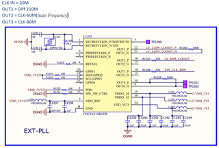
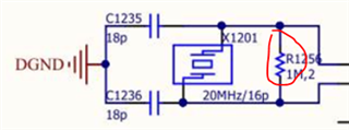
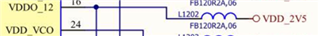
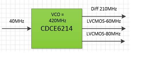
Here is the design block with CDCE6214 for FPGA usage in HMI application.
Could you check if this topology is ok or other suggestions? Very thanks.
Regards
Brian W
Part Number: CDCE6214
Here is the design block with CDCE6214 for FPGA usage in HMI application.
Could you check if this topology is ok or other suggestions? Very thanks.
Regards
Brian W