


Other Parts Discussed in Thread: CD4060B
Hi,
I would like to make, based on TLC555ID chip, an astable operation design with following output characteristics:
- Tlow = Thigh = ~3s
- Tperiod = 6s (duty cycle ~50%)
I calculate values for components, as shown below:
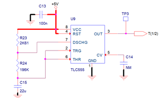
These calculated values are confirmed by Tina Simulation (I downloaded Astable reference design available on TI site).
The problem is that in reality I do not have the required output period (Tperiod = 3s instead of 6s, duty cycle is OK):
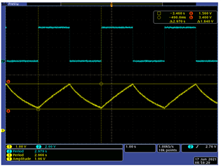
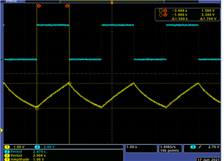
Yellow curve is voltage on C15 (pins 2/6).
Blue curve is output voltage (pin 3)
I understand that C15 tolerance (20%) can influence but not in a 50% ratio (R23/24 are 1% tolerance).
Does anyone have an idea what is wrong?
Thanks.


