This thread has been locked.

If you have a related question, please click the "Ask a related question" button in the top right corner. The newly created question will be automatically linked to this question.

LMX2581E: Issue communicating with LMX2581E

Part Number: LMX2581E

Hello,
I designed a board with an LMX2581E and I can't manage to communicate with it.

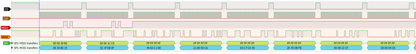
I followed the datasheet recommended initialization sequence which suggest when power is good to soft reset the LMX then write from R15 to R0 the value needed for operation. This is the sequence I'm sending:

0x0020 0015 //R05 - RESET

0x0000 080F //R15
0x4082 000D//R13
0x0008 2437 //R07
============================================
| R7 || Pinmode      | INVERTED | SELECT   |
|----||--------------|----------|----------|
| LD || HD_PUSH_PULL | NORMAL   | READBACK |
| MUX|| PUSH_PULL    | NORMAL   | READBACK |
| FL || TRI_STATE    | NORMAL   | GND      |
============================================
0x0000 00C6//R06
0x0020 0005 //R05
0x0000 0004 //R04
0x0002 FBC3//R03
0x0A00 0002//R02
0x0000 0011 //R01
0x000E 0000 //R00

After writing in R15 Muxout goes and stay at 1 forever, software reset is not sufficient, needs power cycling
The first 2 word received are:
0x0000 1CC0
If I skip R15:
After writing in R13 Muxout goes and stay at 0 forever, software reset is not sufficient, needs power cycling *
The first 2 word received are:
0x0000 1CC0

*Note: If R15 is sent after R13, then Muxout becomes 1

If I skip R13 and R15:
The first 9 words are : 0x0000 1CC0
Then, after writing in R0, it becomes 0x0000 0530

After sending the initialization register (initially R15 to R0 but now R7 to R0), I read all of them using R6: 0x0000 01E6 ... 0x0000 0006
and the value always stay at 0x0000 0530

All of this is repeated a few time and checked using a logic analyzer. It seems that the chip is responding but not how I expect it. I think this could be the diagnostic readback, but it seems odd since it doesn't comply with Fig.18 (p.22) of the datasheet where it should be 0xXXXX XXXF (address should be 1's)

It's also behave oddly since when I change R7 and invert Muxout or change Select, the result is the same. So I don't think the LMX2581E understand what I'm saying. But on the other hand, I don't see why not. My schematic is pretty much the same to the demo board.

Do you have any clue what I might do wrong?

Thanks

  • Hi Julien,

    Could you use TICS Pro to setup your configuration and then cross check the register values with your own software? This will ensure you will program the correct register values. 

    In addition, did you write R10, R9 and R8? 

  • Hello Noel,

    I used the software as suggested. The values are a bit different due to the "read only bit" of the different registers.

    No I wasn't programming R10,R9 and R8 because they are all read only values. I didn't thought it was required to program them.

    This is my updated sequence:

    0x00308015 // Rest

    0x021F E80F //R15
    0x4082 C10D //R13
    0x2100 50CA //R10
    0x03C7 C039 //R09
    0x207D DBF8 //R08
    0x0008 2337 //R07
    0x0000 04C6 //R06
    0x0030 8005 //R05
    0x0000 0004 //R04
    0x2004 F3E3 //R03
    0x0FD0 9002 //R02
    0xC400 2051 //R01
    0x4087 0000 //R00

    and I receive (simultaneously)

    0x0000 3980  //During reset (0x3980 = 0x1CC0 << 1)
    0x0000 1CC0 //During R15
    0xFFFF FFFF //During R13
    0xFFFF FFFF //During R10 and after
    (...)

    This is the output of my logic analyzer if it can help:

  • Hello Julien,

    A couple thoughts:

    • R10, R9, R8 are not read-only values - see datasheet 8.6.1.3. It is crucial that these registers are programmed.
    • Is the reference oscillator present while programming the device?
    • I can't really see because the image is too small, but are you observing the TCES clock-to-enable setup time of 10ns? It looks like MOSI and rising edge of the clock are transitioning simultaneously... perhaps you could zoom in on the portion of the transaction containing the first two register writes, or even just a single write, along with a timebase which can help verify the timings?
    • The datasheet recommends choosing either LD or MUXOUT as readback. Perhaps this should be interpreted as an XOR? Can you see what happens when only one of these is selected? I don't think this is the problem because programming fails after R15... low priority but I guess something to try.

    Regards,

    Derek Payne

  • Hi Derek,

    • Good to know for R10 to R8. I'll add them to my code.
    • Yes, a 100MHz oscillator is powered on and stabilized on OSCIN before sending the reset.
    • You have good eyes! Yes, MOSI is changing on rising edge and should be read on falling clock. I was confused since the MUXOUT should be read on falling edge according to figure 18 (8.3.14.2). My logic analyzer is not good enough to measure such small differences but after checking it on a scope, the clock to enable setup time is much lower then 10ns. Probably more like 500ps. I'll try to fix that.
    • Regarding LD and Muxout being the same, I changed it (surprise, surprise didn't changed a thing!

    I'll try to fix the timing issue and post the results.

    Thanks

  • Hi Derek,

    you found it, that was the issue!

    Thanks

    Julien

  • Excellent, glad I could help!

    Regards,

    Derek Payne