This thread has been locked.

If you have a related question, please click the "Ask a related question" button in the top right corner. The newly created question will be automatically linked to this question.

LMK04828: High frequency noise on SPI signals

Part Number: LMK04828
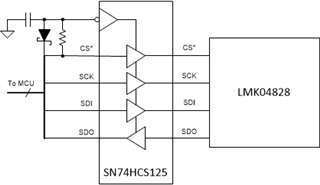
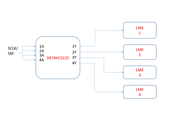
Other Parts Discussed in Thread: SN74HCS125

Hello,

Could you please suggest techniques to mitigate high frequency noise on SPI lines. The details are below - 

SPI frequency - 20MHz

Noise frequency ~1GHz @ -30dBc

Can we add RC filter for each SPI pin and place it close to the IC ? If yes, are there any drawbacks to this ?

  • Hello RajK,

    Yes, you can use an RC filter for the SPI pins to roll off higher order harmonics. The major concern is making sure that you can meet VIH/VIL requirements at 20MHz with your filter in place. However, at 20MHz the fundamental and close harmonics are in a somewhat difficult band to eliminate entirely by any means: if you filter it too much, you cannot achieve SPI frequency; but there is limited capability for the power supplies on the LMK04828 to filter signals between 10-100MHz.

    Additionally, you should decouple the digital supply with a capacitor that has low impedance at 20MHz, and you should separate noise-sensitive supplies such as VCC9_CP2 and the VCC1_VCO. While our power recommendations suggest that it is usually possible to tie the VCO supply to the digital supply without issue because of the limited current draw and signals on this supply, if the SPI clock is running at 20MHz during clocking operation the assumption becomes invalid. The VCO supply has internal LDOs, but the bandwidth of the control loop in the LDO is not high enough to reject SPI >10MHz very well. Isolating the VCO supply from the digital supply helps a little, but most ferrite beads do not have good rejection at 10MHz to 100MHz range.

    A better option for performance, though adding cost and space, is a buffer with OE* tied to CS*, such as SN74HCS125. You could put a small R-C-diode filter on the OE* pin connection (for fast L and delayed H condition) and drive both OE* and one of the buffers with the CS* signal. This would isolate the LMK04828 from SPI entirely when not in use, including the clock. 

    Regards,

    Derek Payne

  • Hi Derek,

    Thank you for the detailed response. We can drop the SPI frequency well below 10MHz (1MHz or below) and use RC filter since the LMK chip is configured only once at the start of operation and the SPI lines are silent for the rest of the time. 

    OR

    We can still operate SPI at 20MHz and use SN74HCS125 as a buffer between FPGA and LMK. Do you have part and footprint recommendations for the RC diode filter components ? Can one SN74HCS125 be used for 4 LMK chips since all of them share the clock and data line as shown below 


    With both these techniques, will there be any concern for the rise times of SPI signals ?

  • RajK,

    Maybe I'm misunderstanding something. Are you saying that you can cease all SPI transactions system-wide after configuring the LMK, i.e. you have no other devices on the SPI bus or you are not actively communicating with other devices on the SPI bus after LMK is configured? If that's the case, then disabling the SPI clock is by itself sufficient. If there is no SPI clock running simultaneously with the LMK clocks, there is no noise coupling. These noise mitigation techniques should only really be required if the SPI bus is active while the LMK clocking signals are active.

    Assuming you still have need to prevent the SPI signals from corrupting the LMK clocks during operation:

    If you can run at lower frequency like 1MHz, this allows the filter to cut off higher order harmonics above 10MHz and the device LDOs will help reject noise at lower frequencies. This should have no concerns with SPI rise/fall time, since the first few harmonics will still be present in the 1MHz signal and the waveform can still retain a relatively square shape. The filters could be applied to the LMK SPI lines regardless of whether they are driven by SN74HCS125 or some other bus controller.

    The point of putting the SN74HCS125 in between the bus controller and the LMK is to force the output of the driver into Hi-Z when the chip select signal is present. So for example, if you expect to program one LMK while another LMK is running, and you do not want the SPI bus to add noise to the operating LMK, the scheme as drawn does not make sense, since the chip select would be duplicated for all four devices. On the other hand, if you expect to program all the LMKs at once with the same configuration, and you have other devices elsewhere on the SPI bus that need to be programmed (with a separate chip select), the SN74HCS125 prevents the SPI signals from reaching the LMKs unless the LMK chip select signal is pulled low. If there are no other devices on the SPI bus, and no further SPI transactions, the SN74HCS125 is superfluous and can be omitted.

    If the SN74HCS125 is used, you must include weak pull-up or pull-down component to the SPI lines (SCK/SDI: pull-down; CS*: pull-up, maybe 10kΩ, just one per SN74HCS125 output), to ensure that the SPI bus does not spontaneously begin toggling with Hi-Z drive. It will not influence the overall drive strength of the SN74HCS125 with such a small value, but it will maintain a stable DC value on the SPI inputs.

    If the SN74HCS125 is used, you would design the R-C-diode network such that the RC time constant to go high at the OE* pin is a few SPI clock periods - long enough to allow back-to-back SPI writes without disabling the driver, but short enough that it does not wait long to write to other non-LMK devices if needed. R-C-diode components don't need to be physically large; use a relatively small capacitor e.g. <1nF to reduce the capacitor footprint, diode size, and bus controller drive strength required to pull CS* low quickly; resistor values large enough for this network can be found in standard package sizes down to 0201.

    Regards,

    Derek Payne