This thread has been locked.

If you have a related question, please click the "Ask a related question" button in the top right corner. The newly created question will be automatically linked to this question.

LMX2820: SPI protocol details needed

Part Number: LMX2820
Other Parts Discussed in Thread: LMX2594

Team, 

My customer is working on a design where FPGA is interfacing to the LMX2820 and is am having trouble finding any information on the SPI interface.

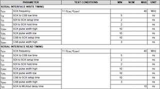
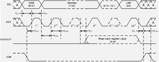
The data sheet contains the timing parameters, but not a timing diagram or even a description of what the protocol is. Specifically, he needs to know what position / how many address bits, Read / Write Bit, and Data bits in a SPI transaction.

Thanks!

Viktorija

  • Hi Viktorija,

    SPI is same as LMX2594, here is the details.

    Register structure

    • The LMX2820 is programmed using 24-bit shift registers.
    • The shift register consists of a R/W bit (MSB), followed by a 7-bit address field and a 16-bit data field. For the R/W bit, 0 is for write, and 1 is for read.
    • Serial data is shifted MSB first into the shift register.

    Programming notes

    • To write registers:

    –The R/W bit must be set to 0.

    –The data on SDI pin is clocked into the shift register upon the rising edge of the clocks on SCK pin. On the rising edge of the 24th clock cycle, the data is transferred from the data field into the selected register bank.

    –The CS# pin may be held high after programming, which causes the LMX2820 to ignore clock pulses.

    –If the SCK and SDI lines are toggled while the VCO is in lock, as is sometimes the case when these lines are shared between devices, the phase noise may be degraded during the time of this programming.

    • To read back registers:

    –The R/W bit must be set to 1.

    –The data field contents on the SDI line are ignored.

    –The read back data on MUXOUT pin is clocked out starting from the falling edge of the 8th clock cycle.

    Programming – initial power-up sequence

    1.Apply power to the device.

    –When power is initially applied, the Power-on Reset (POR) circuitry will reset the registers and state machines to a default state

    2.Program RESET = 1 to reset registers.

    –Although the POR circuitry does initialize the device, it is good practice to toggle the RESET bit from 1 to 0 to manually do a software reset. This is necessary to ensure that the internal state machines, bias levels, and overall device current reset to a stable starting condition

    3.Program RESET = 0 to remove reset.

    4.Program the registers in descending order; R0 should be the last register programmed

    5.Wait 10 ms to allow the internal LDOs to fully power up.

    6.Program R0 register one more time to activate the VCO calibration with the LDOs in a stable state.

  • Thank you, Noel. This addresses my customer's questions. 

    Please consider adding this information to the datasheet. 

    Thanks

    Viktorija