A related question is a question created from another question. When the related question is created, it will be automatically linked to the original question.
If you have a related question, please click the "Ask a related question" button in the top right corner. The newly created question will be automatically linked to this question.
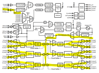
You would set the MODE field to clock distribution mode (R11[31:27] = 0x10). Then, the input on CLKin1 will be routed to the clock distribution path. However, this will only reach the 12 outputs that are available on the clock distribution path. The OSCout0 and OSCout1 outputs will not be accessible from the clock distribution path.
You may want to take a look at the clock buffers portfolio, including the LMK01801 specifically. LMK01801 is a lower cost dedicated buffer/divider.