This thread has been locked.

If you have a related question, please click the "Ask a related question" button in the top right corner. The newly created question will be automatically linked to this question.

LMK04828: CLKin0/0* inputs

Part Number: LMK04828

Hi All, 

I have a question regarding CLKin0/0* input in the LMK04828:

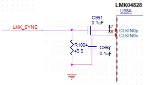
We drive it via AC coupling and in its MOS mode (CLKinX_TYPE=1).

CLKin0* is connected via a capacitor to GND.


We would like to bias it correctly, so when there is no activity on CLKin0/0* (AC coupling capacitors are in cut-off), there will be no false triggering (noise, etc.).

I don’t think I am allowed to connect a PU and PD on CLKin0 and CLKin0* respectively, since |VCLKinX-offset| states 55mV typical between these pins.

How should we handle this situation of biasing the inputs correctly for a no-activity situation?


Thank you!

Gil

  • Hi Gil,

    The most straightforward way is generally to provide a DC-coupled input. The typical CLKinX offset is a self-bias level generated through ~20-50kΩ impedances. With a DC input source the default bias can easily be overridden. However, this prevents the use of LOS detection, which may not be an option; and the signal swing requirements increase greatly, as DC-coupled input is designed for 2.5V or 3.3V LVCMOS inputs.

    If AC coupling is required or preferred, the built-in offset should bias the pins to a static state - no further changes can be made without greatly impacting signal integrity. When the input is AC-coupled through 0.1µF capacitors, the AC-coupling cutoff is very low (~100Hz); any signal coupling onto the CLKin0 input path by more than ~50mV can cause the input stage to toggle, including 50mV ground noise between AC-coupling capacitor and DAP grounding. In practice, assuming common-mode noise can be effectively mitigated with continuous local ground plane at a common voltage between AC-coupling and DAP ground, the 50Ω termination to ground on the input path requires a spontaneous 1mA current to develop on the CLKin0 signal path before a 50mV signal is observed. If such a signal can be generated spuriously in your design, you might consider burying the CLKin0 routing between copper planes. The remaining portion of the signal after the AC-coupling is still high-impedance and could be susceptible to coupled signals, but the trace length is small enough that capacitive or antenna coupling effects will be minimal.

    You can also configure CLKin0_OUT_MUX to the OFF state, ensuring that no signal on CLKin0 propagates through the CLKin0 output. This does not prevent the CLKin0 stage from toggling, and it does not prevent CLKin0 oscillation from coupling onto CLKin1 path as a spur through the power supply, but reducing the path length and number of stages in the device which are carrying or repeating the CLKin0 signal will minimize the coupling and the spurious effects from CLKin0 path.

    Regards,

    Derek Payne

  • hello Derek,

    Thank you for a detailed reply.

    1. We require AC coupling and are using the MOS mode (CLKinX_TYPE=1).

    It proved to be better for us (I think with regard to phase-noise performance).

    1mA (on the 50ohm) is considered high when it comes to noise, plus it should have minimum energy/duration to affect the input stage.

    I don't see that happening in our design.

    In addition, the 50ohm and AC coupling capacitor are located close to device pin, so noise traces coupling is very unlikely to happen.

    So, are we out of danger here?

    2. If we still decide to add a PU/PD on both inputs, what is the DC offset, between the inputs, that is allowed here?

    What value of PU/PD can we use? (considering the internal self-bias levels that are produced inside the device).

    3. With regard to the input circuit for CLKin0/0*: what is the difference between bipolar and MOS modes?

    Thank you!

    Gil

  • Hi Gil,

    Apologies for the delay... we had some E2E backend updates that mixed up assignments.

    So, are we out of danger here?

    Sounds like yes to me.

    2. If we still decide to add a PU/PD on both inputs, what is the DC offset, between the inputs, that is allowed here?

    What value of PU/PD can we use? (considering the internal self-bias levels that are produced inside the device).

    In MOS mode, the inputs can be DC-coupled, so the DC bias can be as wide as you want... as long as you still have the ability to cross the differential positive/negative threshold. I'd recommend something like 50mV to 100mV hysteresis from PU/PD combination < 5kΩ sum. If you want, you could make it so the PU || PD equivalent is 50Ω single-ended termination, but this will draw a lot of DC current to maintain the bias levels.

    3. With regard to the input circuit for CLKin0/0*: what is the difference between bipolar and MOS modes?
    • Normally in bipolar mode there's a set of three anti-parallel diodes across the input pins internal to the device, to clamp the differential input swing and prevent the inputs from saturating or getting damaged. Bipolar mode is internally AC-coupled with ~1pF, and VCM is set to a nominal 1.65V with a biasing PU/PD resistor pair in the 50kΩ range. In theory you don't strictly need to AC-couple bipolar mode, but DC-coupled signals should match the nominal 1.65V VCM set by the internal biasing to prevent saturating the differential pair with large signals; all of our simulations and validation were performed with the external AC-coupling caps. OSCin is hard-coded to bipolar mode. Bipolar mode noise floor and 1/f is slightly better overall just due to BJT vs MOSFET device physics - maybe a few dB total.
    • MOS mode supports DC-coupling for signal types like LVCMOS. Technically MOS mode has internal AC-coupling from the gate of the MOSFET in the input differential pair, but we don't treat this as "AC-coupled" in the datasheet. MOS mode is also biased to a nominal 1.65V VCM. In DC-coupled configuration, the biasing structure can be easily overridden by a low-impedance source (e.g. an LVCMOS output). MOS mode also supports external AC-coupling. 1/f and noise floor performance is a little worse than bipolar, but most of the time this is okay since the clock input is cleaned by the VCXO PLL.
    • You can only use LOS detection in MOS mode, and it has to be AC-coupled with no external biasing at the pins to work correctly. This comes down to DC input current sensitivity at the LOS detector throwing off the results.
    • MOS mode is typically preferred for DC-coupling LVCMOS-based SYSREF or some kind of single-ended CMOS SYNC signal, from CLKin0 to the SYNC/SYSREF subsystem, specifically because it avoids all the problems you brought up at the start of the thread for timing-precise signals.

    Regards,

    Derek Payne