This thread has been locked.

If you have a related question, please click the "Ask a related question" button in the top right corner. The newly created question will be automatically linked to this question.

LMK04828: PLL1 Not Locking at Package Temp above 36°C , PLL1_DLD Oscillates

Part Number: LMK04828

Overview

Our LMK04828 design intermittently fails PLL1 initial lock at startup. We are able to reproduce this failure if the LMK is “pre-warmed” up to a package temp of about 36°C from the last power cycle. If we power it up and the LMK’s package temp is ambient 25°C, the LMK achieves PLL1 lock and never loses lock, even if the package heats beyond 36°C. In the failed lock condition, PLL1_DLD, CP1Out, and the digital IO oscillate at some multiple of MHz frequency. We are seeking support from a TI engineer as the behavior seems to be not defined in the datasheet, and have provided the circuit schematic, LMK register settings, and scope shots.
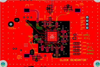
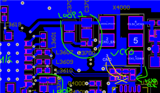
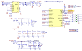
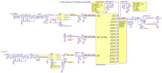
Schematic Design

LMK Register Settings

CurrentSettings.txt
R0 (INIT)	0x000090
R0	0x000010
R2	0x000200
R3	0x000306
R4	0x0004D0
R5	0x00055B
R6	0x000600
R12	0x000C51
R13	0x000D04
R256	0x01007E
R257	0x010122
R258	0x010255
R259	0x010305
R260	0x010462
R261	0x010500
R262	0x0106B0
R263	0x010706
R264	0x010868
R265	0x010922
R266	0x010A55
R267	0x010B05
R268	0x010C62
R269	0x010D00
R270	0x010EB0
R271	0x010F16
R272	0x01107E
R273	0x011122
R274	0x011255
R275	0x011305
R276	0x011462
R277	0x011500
R278	0x0116B0
R279	0x011706
R280	0x011861
R281	0x011955
R282	0x011A55
R283	0x011B01
R284	0x011C22
R285	0x011D00
R286	0x011E70
R287	0x011F06
R288	0x01200A
R289	0x012155
R290	0x012255
R291	0x012300
R292	0x012422
R293	0x012500
R294	0x012670
R295	0x012711
R296	0x012868
R297	0x012922
R298	0x012A55
R299	0x012B05
R300	0x012C62
R301	0x012D00
R302	0x012EB0
R303	0x012F11
R304	0x01301E
R305	0x013122
R306	0x013255
R307	0x013305
R308	0x013442
R309	0x013500
R310	0x0136B0
R311	0x013761
R312	0x013830
R313	0x013903
R314	0x013A02
R315	0x013B80
R316	0x013C00
R317	0x013D08
R318	0x013E03
R319	0x013F00
R320	0x014000
R321	0x014100
R322	0x014200
R323	0x014311
R324	0x0144FF
R325	0x01457F
R326	0x014608
R327	0x01470E
R328	0x014813
R329	0x014913
R330	0x014A00
R331	0x014B05
R332	0x014CFF
R333	0x014D00
R334	0x014E00
R335	0x014F7F
R336	0x015000
R337	0x015102
R338	0x015200
R339	0x015300
R340	0x015401
R341	0x015500
R342	0x015601
R343	0x015700
R344	0x01580A
R345	0x015900
R346	0x015A0A
R347	0x015BDF
R348	0x015C20
R349	0x015D00
R350	0x015E00
R351	0x015F0B
R352	0x016000
R353	0x01610A
R354	0x016290
R355	0x016300
R356	0x016400
R357	0x016504
R369	0x0171AA
R370	0x017202
R380	0x017C15
R381	0x017D33
R358	0x016600
R359	0x016700
R360	0x01684B
R361	0x016949
R362	0x016A00
R363	0x016B20
R364	0x016C00
R365	0x016D00
R366	0x016E13
R371	0x017300
R386	0x018200
R387	0x018300
R388	0x018400
R389	0x018500
R392	0x018800
R393	0x018900
R394	0x018A00
R395	0x018B00
R8189	0x1FFD00
R8190	0x1FFE00
R8191	0x1FFF53

Experiments

We started by determining the condition in which PLL1 goes unstable and does not lock. The failure seemed temperature dependent so we began by cooling IC’s with canned air in an attempt to find which IC is sensitive and where the threshold is. We found that when the LMK04828’s package starts above 36°C and the LMK is powered on, PLL1 will not lock. This test was repeated with a hot board and a small heat gun, warming the IC. Interestingly, if the LMK is powered on while it is cold it locks instantly and maintains lock well above 36°C.

When the LMK fails to lock, the Status_LD1 I/O assigned to the PLL1_DLD lock state oscillates at either 100MHz, 10MHz, 5MHz or other whole number divisions of 100MHz. With our PLL1_WND_SIZE set to 43ns and PLL1_DLD_CNT set to 8192 we don't believe the LD1 PLL1 lock output should be able to switch states at anywhere near these frequencies if the datasheet is correct. We worry that the LMK is entering an undefined state or a feedback loop, of which we have no clear solution. It feels pertinent to note that in this state the LMK’s digital outputs and inputs (SPI and LD1/LD2) have significant noise present at the same frequency when in the fault condition.

We have checked the LMK’s 3V3 supply, it is clean and provided by a local low noise LDO (TPS7A4701). The filtering into the VCC pins for the various supplies on the LMK are decoupled with appropriate capacitors and filtered with appropriate low series resistance ferrites. The decoupling scheme to our knowledge aligns with the recommendations in the datasheet. We additionally tried powering the VCXO from a different supply than the LMK’s supply and found the same behavior was present.

Our reference OCXO (±50ppb) is powered from another separate LDO supply and conforms to slew rate and voltage requirements. Our VCXO (±50ppm absolute pulling range) also conforms to slew and output voltage requirements. It has a max pulling range of 50ppm and in normal operation does not thermally drift more than 18ppm (calculated by differencing the hot and cold PLL1 control voltage as well as the ppm/V values).

We have attempted multiple loop filter R C configurations for bandwidths, 100hz, 1000hz, and 20khz (the schematic shows Loop Filter PLL1 for 100hz). All calculated with the PLLatinum Sim. The response of the PLL seems appropriately damped when it manages to lock, leading us to believe our loop filter is appropriately tuned.

We have disabled the reset input in an attempt to remove the possibility of it responding to noise and resetting the LMK. We have holdover disabled, PLL delays disabled, and no sync or clock source switching enabled. We tried lowering PLL1’s detect frequency from 10Mhz to 1Mhz with a divider change and found the same fault. We also tried powering down the entire DCLK/SDCLK output stage and found the same fault.

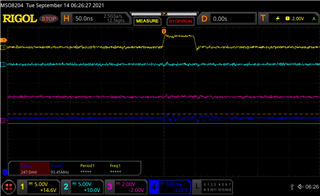
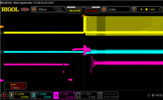
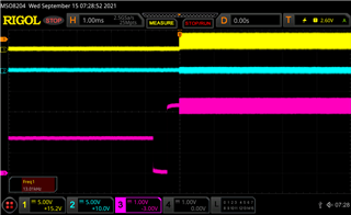
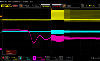
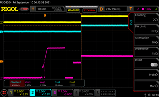
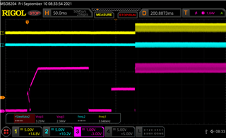
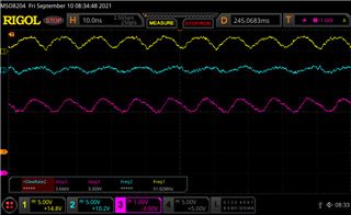
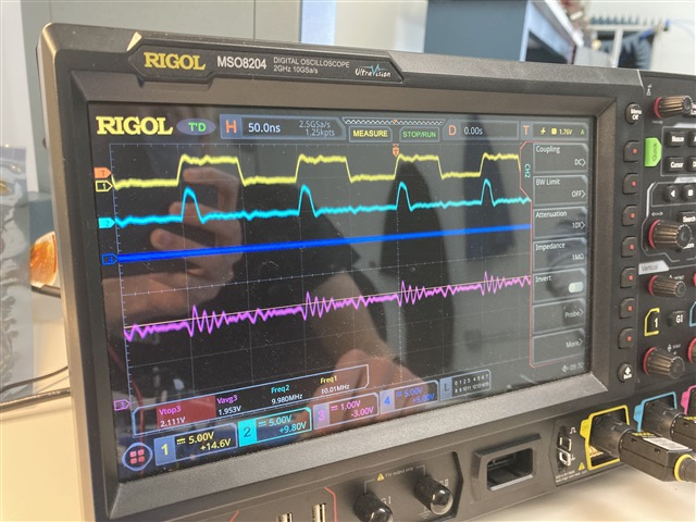
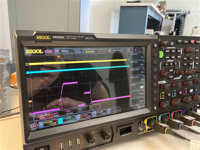
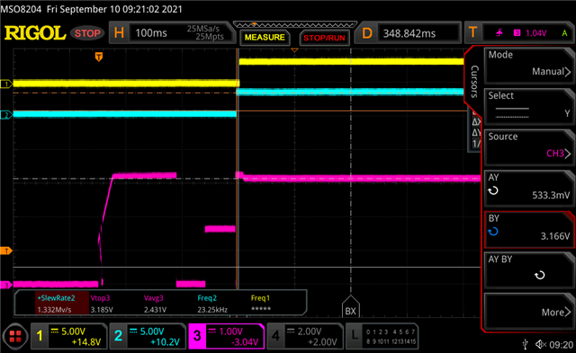
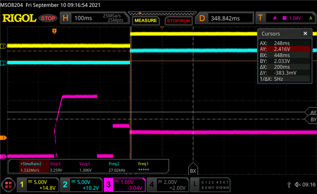
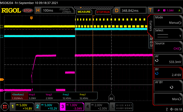
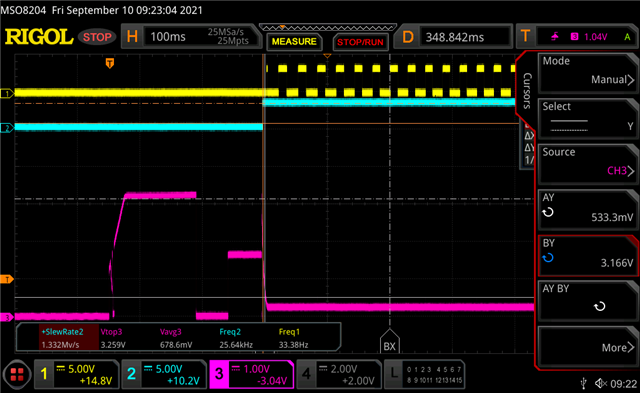
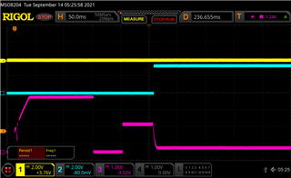
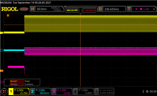
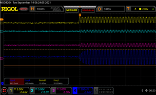
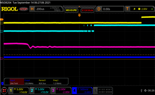
For all Scope Captures:

Trace 1 - LD1(PLL1 lock)

Trace 2 - LD2(PLL2 lock)

Trace 3 - PLL1 control voltage output

 Capture of a successful lock with a room temperature board (RigolDS0.png)

Failure to Lock (Control voltage drifts up to 3V3) (RigolDS18.png)

Failure to Lock (Control voltage drops to close to 0V) (RigolDS7.png)

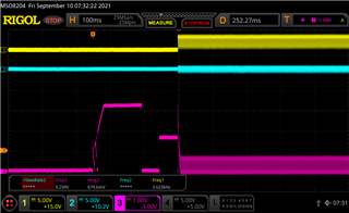
Failure to lock (finer timescale) (RigolDS20.png)

  • Hello Justin,

    Assuming your Kvco is correct, your loop filter looks stable to me. I doubt this is the problem.

    Low probability of being related, but I recommend setting PLL2 N-Cal divider equal to PLL2 N divider, since right now PLL2 VCO range is being calibrated using 3000/16 as the feedback frequency instead of 3000/300. This would usually only affect PLL2, but it eliminates one extra variable.

    As for your PLL1 problem, I can't find anything in your post that says the state of PLL2 lock detect. Since OSCin is used both as the PLL1 feedback and the PLL2 reference, which PLL is failing to lock is usually indicative of the source of your problem. If neither PLL locks, and unrelated misconfigurations of PLL2 have been sorted out (e.g. PLL2 N-Cal divider set incorrectly), this points to something happening at the VCXO; if PLL1 alone is failing to lock, this suggests the reference input is not being adequately captured.

    A helpful tactic for debugging lock issues is monitoring what the reference and feedback paths at the phase detector are seeing. Instead of monitoring PLL1_DLD and PLL2_DLD on the lock detect signals, you can monitor PLL1 R and PLL1 N, and look for a stable signal.

    All this is assuming there is an issue with locking. But based on your post, it sounds possible that there is some other issue happening, since I agree that it sounds implausible for the window detect to be oscillating at the rate described. I'd still be interested to see if the results of PLL1 R/N monitoring suggest the PLL is locking, and this is some state machine issue.

    There is a bit, CLKin_OVERRIDE (R336[6] or 0x150[6]), accessible from the general controls in the user controls page. Can you try setting this to 1? Since you are using register-based selection of CLKin0, this bit may force the state machine into a stable state for clock selection... but I'm not sure why it would be required, other than due to some kind of bug.

    Finally, are you seeing this issue on more than one device?

    Regards,

    Derek Payne

  • Hello Derek,

    First of all thank you for such a quick reply. We appreciate your help.

    With regards to which PLL locks we seem to see three or four different fail states. The first and most common state is shown in the scope captures in Justin's post. We see the lock bit for PLL1 oscillate, but PLL2's lock bit stays low other than the noise we found present on almost all the signals. The chip seems to go into this state most often. When the IC is very hot (45+ degrees C), it almost strictly fails into this mode. We have seen two other failed states; one in which PLL1 does not lock and PLL2 locks, and one in which PLL1 locks and PLL2 remains unlocked. Both of these states are much rarer, and were only seen on occasion (1/20 attempts) and only when the temperature was close to the 34-36 degree cutoff we described. The most common failure, the one we outlined in the first post, shows both PLLs not locking, but PLL1's lock bit oscillating and PLL2's bit remaining low other than noise.

    In response to the N and R signal testing question. We have programmed the LMK to output PLL1's N and R clock signals and captured the response in both successful and failed states.

    Trace 1(yellow) is the R signal, trace 2(blue) is the N signal, and again trace 3(pink) is the VCXO control voltage after the loop filter.

    This capture shows a successful lock of PLL1 as well as PLL2:

    Here is a smaller timescale capture of the same signals:

    We see the two clock signals start out of phase and adjust into phase as the control loop hunts for lock, once the control voltage settles we see the two signals locked as we would expect. I assume the smaller period of the N clock is due to the 10x division occurring after the VCXO and before the phase detector?

    The interesting thing is that when the chip goes into the failure mode we described, the N and R signals are no longer present at the LD1 and LD2 outputs. We were puzzled by this, as we expected the IC to still present the clock signals regardless of lock state. We confirmed that both clock's were still operational and had valid logic levels and slew rates in this state.

    Capture of a failed lock (above threshold temp) showing no N or R clock outputs:

    On a slight tangent, we attempted to validate our capture range of PLL1 out of fear that the VCXO was possible drifting too far to be locked with the reference. We provided an external reference signal to the PLL1 reference input by modifying the CLKin_MUX and connecting a signal generator. We then began increasing and lowering this input references frequency to make force the PLL to have to seek further in the pulling range of the VCXO. With the board cold we saw the PLL successfully lock throughout the control voltages range with reference frequencies deviating 1000Hz or more. We believe this proves that the slight frequency drift we see on the VCXO due to thermals is not a factor in the instability of the LMK. The PLL1 loop is sufficiently tuned to provide a more than adequate capture range. Please advise as to if our testing logic here is valid.

    Trace 1(yellow) is the PLL1 lock signal, trace 2(blue) is the PLL2 lock signal, and again trace 3(pink) is the VCXO control voltage after the loop filter.

    Capture showing the PLL locking at the higher end of the VCXO pulling range:

    Capture showing the PLL locking at the lower end of the VCXO pulling range:


    When the reference was skewed beyond the pulling range of the VCXO we saw lock instability as we would expect. But the failure mode was closer to expectations. Intermittent PLL1 locks as the charge pump reached the limits of the control voltage output.

    Instability as the VCXO is at its upper frequency limit:

    Instability as the VCXO is at its lower frequency limit:

    We are seeing this failure on multiple boards from the same revision. We also have seen this failure on previous revision of the design with the same clock generation circuit. The full code on the package of the chip we have been testing is 94A3ECUG3 K04828BISQ.

    Thank you again,

    Spencer

  • Spencer,

    It is quite surprising to me to discover that there is no clock signal at all while the device is in the anomalous state. If nothing else, the R-clock should be present as long as there is a reference selection forced. The fact that you can lose both R/N clocks at some temperature threshold suggests there's something going on unrelated to the PLL behavior, like the logic circuit is failing or losing power above some temperature.

    I assume the smaller period of the N clock is due to the 10x division occurring after the VCXO and before the phase detector?

    Yes, the phase detector looks at edges so duty cycle after the divider isn't critical.

    Please advise as to if our testing logic here is valid.

    This experiment makes sense, and as far as I'm concerned it rules out the VCXO pull range as an issue.

    We are seeing this failure on multiple boards from the same revision. We also have seen this failure on previous revision of the design with the same clock generation circuit.

    This is also quite surprising, and leads me to assume that there is something systemically wrong common to both revisions of the design.

    Follow-up questions:

    • If you configure the startup programming such that PLL1 is powered down completely, does PLL2 lock consistently at hot temperature?
    • I didn't see you mention it, did you try this test with the CLKin_OVERRIDE bit set?
    • When probing the supply lines, did you probe the pin voltages on the package, or somewhere nearby e.g. after the ferrite? I am wondering if something is preventing the part from soldering to the board, and you have intermittent contact on one of the supply rails.
    • Is it possible for me to see the layout of the clock generator circuit?

    Regards,

    Derek Payne

  • Hi Derek,

    Thanks for your continued support. We ran the suggested test cases, and continued to see the same dependency on temperature.

    If you configure the startup programming such that PLL1 is powered down completely, does PLL2 lock consistently at hot temperature?

    No. With PLL1 powered down and CPOUT1 tri-stated such that PLL2 uses the raw VCXO as its reference, the LMK continues to exhibit the same behavior of PLL2 locking (observed with LD2 = 1, LD1 = 0) at cold boot, and funky oscillations on LD1 and LD2 at hot boot.

    The first image below is of a successful PLL2 lock at cold with PLL1 disabled. Yellow = PLL1 Lock, Teal = PLL2 Lock, Pink = CPOUT1 (tri-stated).

    The second image is of an unsuccessful PLL2 lock at hot boot and the same register configs. Yellow = PLL1 Lock (expect to be 0, but oscillates up to VCC). Teal = PLL2 lock, Pink = CPOUT1 (expect to be tri-stated but is similarly oscillating).

    I didn't see you mention it, did you try this test with the CLKin_OVERRIDE bit set?

    We attempted the CLKin_Override bit set to 1 and continued to see the same behavior.

    When probing the supply lines, did you probe the pin voltages on the package, or somewhere nearby e.g. after the ferrite? I am wondering if something is preventing the part from soldering to the board, and you have intermittent contact on one of the supply rails.

    Here is a probed supply line after the ferrite (VCC11_CG3) in the fail state. In the fail state, VCC looks really, really bad at 3.3Vdc with 1Vpp swing, though I'm not sure if this is a shortcoming of the supply itself, or the LMK chip is clamping the supply due to a hot fail state. Yellow = PLL1 Lock, Teal = PLL2 Lock, Pink = CPOUT1, Dark Blue = VCC11_CG3

    During the successful cold lock state, the same point probed is at 3.3Vdc and much quieter. It does still seem to get noisy under activity (250mVpp) before PLL1 is fully locked. Pic 1 = Zoomed out, Pic 2 = zoomed in on first trigger of PLL1 Lock.

     .

    Our next test in this category will be to retest with external power sourced to the LMK and VCXO (essentially bypassing the TPS7A4701 LDO), and depending on results, may dead bug a higher capacity LDO to eliminate chance of brownout. In our TICS model, the LMK draws 630mA, while the LDO is sized for 1A output.

    Is it possible for me to see the layout of the clock generator circuit?

    Top Side Layout:

    Bottom Side Layout:

    Another tangent: we determined that the cause of seeing oscillations at 5MHz or 10MHz was due to aliasing on the scope. All the oscillations in the fail state have a 100MHz frequency.

  • Justin,

    I am coming up with closer to 800-870mA depending on VCXO load and LVPECL termination, so I think swapping the LDO with a higher-current supply is a reasonable next-step. I don't know what the OCXO current is, but with 870mA from the clock generator and the OCXO seemingly on the same 3.3V LDO, I wouldn't be surprised if the current limit is being tripped.

    If possible, you could try a simpler register-based test where the CLKOUTs are all powered down. Setting every CLKoutX_Y_PD=1 on powerup cuts the current by ~500mA. You wouldn't have output clocks, but you don't need output clocks to evaluate if the PLL locks successfully in the lower-current condition. You could also monitor the LDO current with all outputs configured for powerdown, and if this number + 500mA > LDO current limit, it is likely the current limit is the culprit.

    The only other thing I could think of is the placement of the 50Ω termination for the VCXO might be injecting some 100MHz noise into the LDO ground. The LDO datasheet makes a somewhat vague statement that no voltage other than GND should be connected to the voltage programming pins, so I wonder if 100MHz ground noise is coupling into one or more of these voltage-setting pins and causing the LDO to rapidly cycle between certain output voltage settings.

    Regards,

    Derek Payne

  • Hi Derek, thanks for the suggestions. As advised, we tested power supplies, with the following starting assumptions:

    The OCXO is powered by an independent 3A LDO and is operating well within the spec of that LDO.

    The LMK and VCXO did share the same TPS7A4701 1A LDO shown earlier in the schematic.

    We shared the same observation as you on the 50Ω GND termination of the VCXO to OSCIN potentially injecting local 100MHz noise into the LDO’s GND, so we attempted this rework, shown in Yellow below, where we “tombstoned” the termination cap and resistor and routed back to the VCXO’s GND. This did not change the performance of the PLL.

    We also tried a number of test cases to rule out current limiting the TPS7A4701 1A LDO:

    1. Fed external 5V at the input of the LDO so that we could monitor the total current of the LMK + VCXO. Total current going into LMK + VCXO was observed to be 700mA at max load.

    2. Disabling all the CLKOUTs and SDCLKOUTs with register settings. We did not obtain a current measurement here, but the LMK’s PLL lock behavior continued to track to temperature.

    3. Replaced the VCXO part with one that draws less current, and has the same frequency stability, pull ratio, slew rate. LMK PLL lock behavior continued to track to temperature.

    4. Replaced the 1A LDO with a 1.5A LDO dead-bugged onto the PCB with extra decoupling. LMK PLL lock behavior continued to track to temperature. We did get a new occasional failure mode after the LDO change in which the LMK continues to run the CPOUT1 loop (Pink) even after the PLL1_DLD (yellow) and PLL2_DLD (blue) start oscillating.

    At other times even with the LDO rework, the LMK did not enter the control loop during the DLD oscillations, matching previous results.

    Lastly, we removed the LMK part (original lot code: 94A3ECUG3 K04828BISQ) and re-soldered a different lot code (0AAKRFUG3 K04828BISQ) part onto the board. Even with the new part installed, the LMK continued to successfully lock at cold and not at hot.

    One last tangent: we confirmed that some of the oscillations on the LMK’s digital lines were in fact NOT scope aliasing as we believed yesterday. We set the trigger on CH1 (STATUS_LD1), and an LMK in the hot mode did oscillate at 3 different frequencies, as shown below.

    Thank you again for your continued support, Derek.

  • Justin,

    This is quite bewildering. Let me run it past a few other people internally in case they've ever heard of anything like this.

    Regards,

    Derek Payne

  • Justin,

    After discussion, there's a few things we're thinking could be at issue, related to somehow triggering a reset event or a supply brownout.

    • The RESET pin connection is not shown, so I'm not sure what's driving it (MCU? Tied high/low elsewhere?). We could try disconnecting the RESET pin and configuring the RESET_TYPE as an output. This eliminates one major path for resets on the device.
    • I notice that the capacitors after the ferrite beads for Vcc7/8/9 are omitted, but footprints for these capacitors are present. Has anyone tested populating these capacitors? There is a bullet point in the datasheet for section 11.1.1.1 which suggests frequencies >30MHz can use the ferrite bead with internal capacitance, but considering the supply voltage ripple on the other supply pins, that capacitance may be required for some high-current portion of a reset event that was overlooked.
      • Our EVMs actually do populate these capacitors, despite a default VCXO frequency of 122.88MHz. It's possible that the failure mode we're encountering now was never observed because these capacitors were never really omitted.

    If neither of the above remedies makes a difference, can we get a readback attempt from a successful and failed lock case, showing the difference? You may also want to probe the MISO line during the failed lock readback transaction, as I have a suspicion that one or more supplies are browning out and the readback may not be clean SPI data any more.

    Regards,

    Derek Payne

  • Hello Derek,

    We went ahead tested both of your suggestions in the last post, unfortunately to no avail. Adding the DNP'd filter capacitors had no change on the behavior.

    In a previous test we changed the reset line to an internal pulldown mode. In an attempt to ensure this wasn't the issue we also added a stiff external pulldown of 1K as well as a filter capacitor of 0.1uF. Neither of these modifications changed the failure mode of the circuit.

    We will look into getting a SPI read off of the IC while in the failed state. Though I assume it will likely fail due to the chips state, as you mentioned. We have moved forward in our investigation by taking steps to generate a development PCB with multiple layouts of the clock generation circuit as well as some new layouts. Hopefully this will lead us to a discovery regarding the root cause of this instability.

    Thank you again,

    Spencer

  • Spencer,

    Understood. Apologies that we didn't have any great answers for you this time. Let us know if you find anything surprising.

    Regards,

    Derek Payne