This thread has been locked.

If you have a related question, please click the "Ask a related question" button in the top right corner. The newly created question will be automatically linked to this question.

LMK04832: Change the external CLK frequency setting

Part Number: LMK04832


Hi teams,

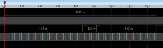
We use NXP Processor to control LMK 04832, its SPI is 4-wired SPI, especially DMA control, the minimum transmission SPI data is 4 bytes (32bits), but LMK04832 programming is 24-bit register, so we fix the programming register at the end One byte is filled with 0.

Will this cause the LMK04832 register to be written abnormally? Please suggest how to handle the communication between different devices of SPI configuration?

The following picture shows writing value 0x90 to register addr 0x00, the bottom is SCK, the top is SDIO, the top is CS, and you can see that should be sent 24-bit (2bytes addr, 1byte data) to SDIO, but NXP Processor's  SPI sent a total of 32-bit data to SDIO.

Thanks.

  • Hello Ryan,

    Although this feature is not documented in the datasheet anywhere, LMK04832 SPI interface is actually designed to process burst write/read mode, so theoretically you should be able to write multiple registers consecutively. Apparently, after the initial 16-bit read/write + address is decoded, every byte read/written with chip select low automatically triggers either an address increment, an address decrement, or an address hold. Assuming you wrote 32 bits, you would have one of three options:

    • Ascending order: e.g. 16 bits r/w and address bits, 8 bits data at register 0x000, 8 bits at register 0x001
    • Descending order: e.g. 16 bits r/w and address bits, 8 bits data at register 0x001, 8 bits at register 0x000
    • Address hold: e.g. 16 bits r/w and address bits, 8 bits data at register 0x000, 8 bits at register 0x000

    The controls for this are handled by R0[2] (ascend/descend) and R0[3] (hold/advance):

    R0[3] R0[2] Behavior of fourth byte
    1 X write/read to same address
    0 1 write/read to address + 1
    0 0 write/read to address - 1

    Although it doesn't say anywhere, I have confirmed that the default for R0 = 0x00 (all zero), which should put you in descending order; this suggests a sequence in which you write to R0 to configure the settings for R0[3:2], let the fourth byte write to 0x7FFF (write will be ignored), then proceed on subsequent writes to use the programmed behavior for the fourth byte. The reset sequence would be slightly complicated since the write with RESET=1 would clear any settings in R0[3:2] to register defaults; so the first write to reset the device and the second write to configure R0[3:2] will always be descending to an ignored address.

    In some cases, you could write to a register that has no clearly defined nearby register in the register map:

    • 0x000 -> 0x001: this is fine, 0x001 is unused (ignored)
    • 0x000 -> 0x7FFF: this is fine, 0x7FFF is unused (ignored)
    • 0x7FFF -> 0x000: this is fine, 0x7FFF is unused (ignored)
    • 0x16E -> 0x16F (R366 -> R367): you must not write 0x16F. Ascending writes should start from 0x16D instead.
    • 0x16E -> 0x16D (R366 -> R365): 0x16D is unused (ignored)
      • As of this comment, the web datasheet appears to have a mistake in the register map: 0x16C is included as all zeros, 0x16D is omitted, and 0x16E is omitted. Instead, 0x16C and 0x16D should be omitted (ignored) and 0x16E should contain PLL2_LD_MUX and PLL2_LD_TYPE fields.
    • 0x173 -> 0x174 (R371 -> R372): 0x174 is unused (ignored)
    • 0x173 -> 0x172 (R371 -> R370): you must not write 0x172. Descending writes should start from 0x174.
    • 0x177 -> either (R375 -> either): ascending/descending burst write is not possible with 32-bit writes as far as I can tell, because you must not write 0x178 or 0x176. set R0[3] = 1 if this field must be accessed.
    • 0x188 -> 0x189 (R392 -> R393): this is fine. 0x189 is read-only, undisclosed device state fields. 
    • 0x555 -> 0x556 (R1365 -> R1366): this is fine, 0x556 is unused (ignored)
    • 0x555 -> 0x554 (R1365 -> R1366): this is fine, 0x554 is unused (ignored)
    • either -> 0x168 (either -> R360): either is fine. Make sure to write 0x173 before writing 0x168 to ensure PLL2_PD and PLL2_PRE_PD are cleared before writing the LSB of the N-divider (which triggers VCO calibration).

    While ascending/descending writes could potentially cut your programming sequence time almost in half, special-casing the ascending/descending writes can understandably add too much complexity. It is simplest from a programming perspective to set R0[3] = 1, then pad the final byte with a duplicate of the data byte.

    Regards,

    Derek Payne