Dear Expert
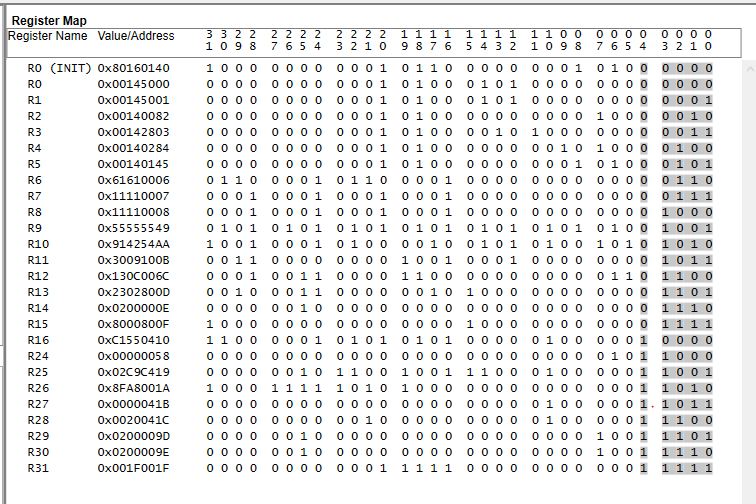
1. The reads and writes of register R0 are inconsistent (write 0x00145000, read back 0x80000320), and the reads and writes of other registers are consistent.The order of writing to register is from top to bottom according to the following table.CLKoutX_Y_DIV and CLKoutX_Y_DDLY can't write to the R0 register.
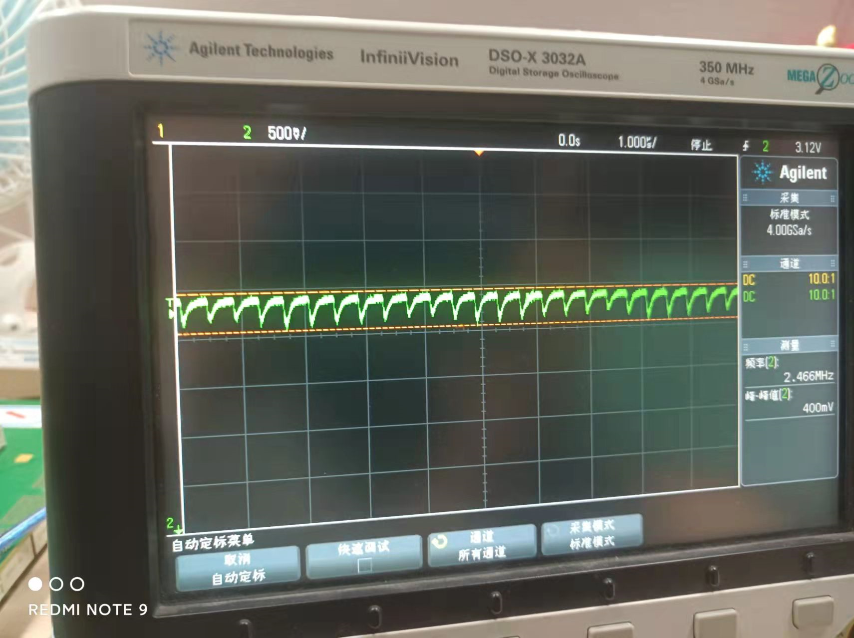
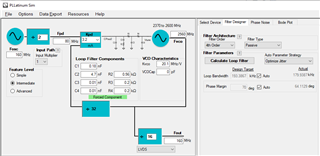
2. PLL often loses lock in 0-delay mode.However, in normal mode, PLL has not yet experienced a loss of lock.There is no difference between the two except register configuration.What is the cause of this?And can the manufacturer give a set of recommended values for C1, C2, R1 (PDF=80MHz)?