It is very common for precision oscillators to output a "clipped sinewave" signal, 0.7 to 0.8V p-p. By removing a high-current rail-to-rail driver from the oscillator package, this reduces self-heating and improves stability.
The standard recommended circuit to convert this to a full amplitude signal is one inverter, one resistor, and one capacitor. Connect the inverter's output to its input through a 1M feedback resistor to bias it to the threshold voltage, and AC-couple the clock signal in through a small capacitor. (Some oscillators have the capacitor built in.)
That's not very many parts, but in my case, the inverter would be an additional line on the BoM that I'd just as soon avoid.
It occurs to me that the inverter with a large feedback resistor is also the standard Pierce crystal driver circuit used by essentially all chips with Xin and Xout pins.
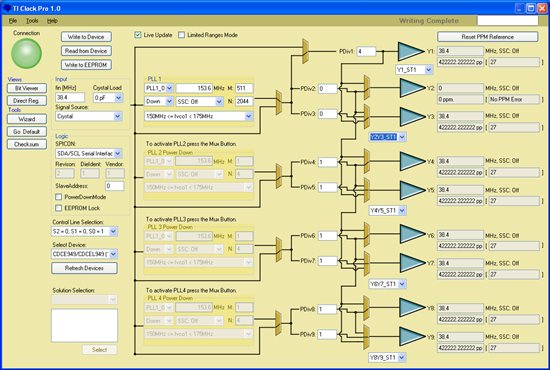
So I should be able to program the CDCE913/925/937/949 input for crystal mode and couple the signal in through a small capacitor; the inverter and feedback resistor are built in.
I'm wondering if this is known to work, or not to work for some reason that escapes me. Or is a different operating mode preferred? I don't know if the feedback bias resistor is connected in LVCMOS input mode.
The oscillator manufacturer thinks it will probably work if the input impedance is high enough. It's 6 pF and an unspecified resistance; I assume it's "plenty high" (> 1MΩ).
Thank you for any advice!