Other Parts Discussed in Thread: CODELOADER
Hi team,
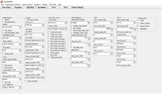
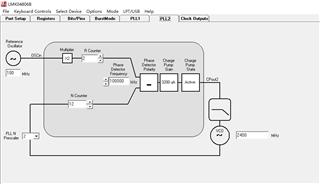
I‘m remote supporting a semiconductor tester project. Customer would like to input a 100MHz OSC to PLL2 through OSCin, powerdown PLL1, and set internal VCO to 2.4G, then divide to 12 channels of clean 100MHz CLKout. They have problem that the HEX configuration attached below doesn't achieve what they want. I can't take an onsite support, but just paper review. Could you pls take a look at the configuration? What I've seen is they should set the phase detector polarity for PLL2 positive.
Thanks.
R0 (INIT)	0x80160140
R0	0x00140300
R1	0x00140301
R2	0x00140302
R3	0x00140303
R4	0x00140304
R5	0x00140305
R6	0x11110006
R7	0x11110007
R8	0x11110008
R9	0x55555549
R10	0x9102410A
R11	0x3000100B
R12	0x0B0C00AC
R13	0x1302080D
R14	0x0200000E
R15	0x8000800F
R16	0xC1550410
R24	0x00000058
R25	0x02C9C419
R26	0xAFA8001A
R27	0x10001E1B
R28	0x00201E1C
R29	0x0180019D
R30	0x0200019E
R31	0x001F001F